

OLED apparatus having improved fault tolerance
- Summary
- Abstract
- Description
- Claims
- Application Information
AI Technical Summary
Benefits of technology
Problems solved by technology
Method used
Image

Examples
first embodiment
[0042] Referring to FIG. 3a, there is shown the present invention, wherein a plurality of electroluminescent diodes 11 are connected in series within each single OLED pixel 10. In this top-emitting configuration, the cathode is transparent. With this arrangement, shorting of one electroluminescent diode 11 simply adds to the current load of the other electroluminescent diode(s) 11 connected in series within OLED pixel 10. Electroluminescent diodes 11 can be themselves the current limiting elements, in which case, each diode 11 within OLED pixel 10 provides some portion of the overall emitted light. Alternately, one or more of the series-connected diodes could be a diode that does not emit light, but simply acts as a current limiting element.
[0043] Referring to FIG. 3b, there is shown a plan view of component positioning within OLED pixel 10 for this first embodiment. Electroluminescent diodes 11 are formed from suitably doped OLED materials and are arranged in series, such that the ...
third embodiment
[0047] Referring to FIG. 5a, there is shown, in schematic form, a third embodiment in which OLED pixel 10 employs a fuse 40 for current limiting. An overcurrent condition caused by shorting of electroluminescent diode 11 would blow fuse 40, effectively causing an open circuit for this OLED pixel 10. A single dark pixel would result; however, other pixels from other OLED pixel 10 would not be affected by this failure. Referring to FIG. 5b, there is shown a plan view of possible component positioning within OLED pixel 10 for this third display embodiment, with fuse 40 connected between the cathode of electroluminescent diode 11 and cathode line 24. It can be appreciated that fuse 40 can alternately be connected between the anode of electroluminescent diode 11 and anode line 26 or between the cathode of electroluminescent diode 11 and cathode line 24. Alternative variations on the embodiment of FIGS. 6a and 6b include series combination of fuse 40 with multiple electroluminescent diode...
fourth embodiment
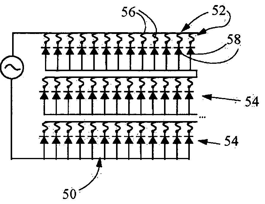
[0055] Referring to FIG. 6a, there is shown the present invention, in which, for any single OLED pixel 10, multiple electroluminescent diodes 11 are disposed electrically in parallel between anode line 26 and cathode line 24, each electroluminescent diode 11 having a separate series fuse 40. With this arrangement, shorting of a single electroluminescent diode 11 blows its corresponding fuse 40, opening this part of the circuit, but permitting continued flow of current through other electroluminescent diodes 11 connected in parallel. Unlike the arrangement of the third display embodiment, however, separate material need not be used to fabricate fuse 40. Instead, the current-carrying capacity of OLED materials themselves, or that of nearby cathode or anode support structures, effectively provides a fusing element with this embodiment. An overcurrent condition melts or bums away conductive material that forms electroluminescent diode 11, opening the circuit at that point.
[0056] Referri...
PUM
 Abstract
Description
Claims
Application Information