Delay circuit with timing adjustment function

a delay circuit and function technology, applied in the field of delay circuits with timing adjustment functions, can solve the problems of inability to maintain locked state, inability to accurately delay input signals, degradation of sensitivity, etc., and achieve the effect of stable timing adjustment and high accuracy

Inactive Publication Date: 2005-08-11
RENESAS ELECTRONICS CORP
View PDF4 Cites 8 Cited by
  • Summary
  • Abstract
  • Description
  • Claims
  • Application Information

AI Technical Summary

Benefits of technology

[0016] The object of the present invention is to provide a delay circuit enabling a stable timing adjustment with high accuracy.

Problems solved by technology

On the other hand, it is difficult to render the characteristics of the elements forming the delay element uniform due to variations in a manufacturing process or fluctuations in the supply voltage or the ambient temperature, and thus, an accurate delay of input signal is undesirably hindered.
For example, when the above-mentioned delay circuit is used for adjusting the timing of each signal in a signal read / write control circuit of DRAM (Dynamic Random-Access Memory), which is based on a row address strobe (RAS) access that uses RAS, the timing of RAS access changes as the set delay time changes, which in turn results in the degradation of the sensitivity.
Practically, however, when the control signal approaches close to the ground voltage level or the supply voltage level, jitter (phase shift) occurs in the generated clock due to the effect of noise superimposed on the supply voltage and the like, and thus the locked state can not be maintained.
Accordingly, with a conventional delay circuit, it has been difficult to perform the timing adjustment stably.

Method used


Image

  • Delay circuit with timing adjustment function
  • Delay circuit with timing adjustment function
  • Delay circuit with timing adjustment function

Examples


first embodiment

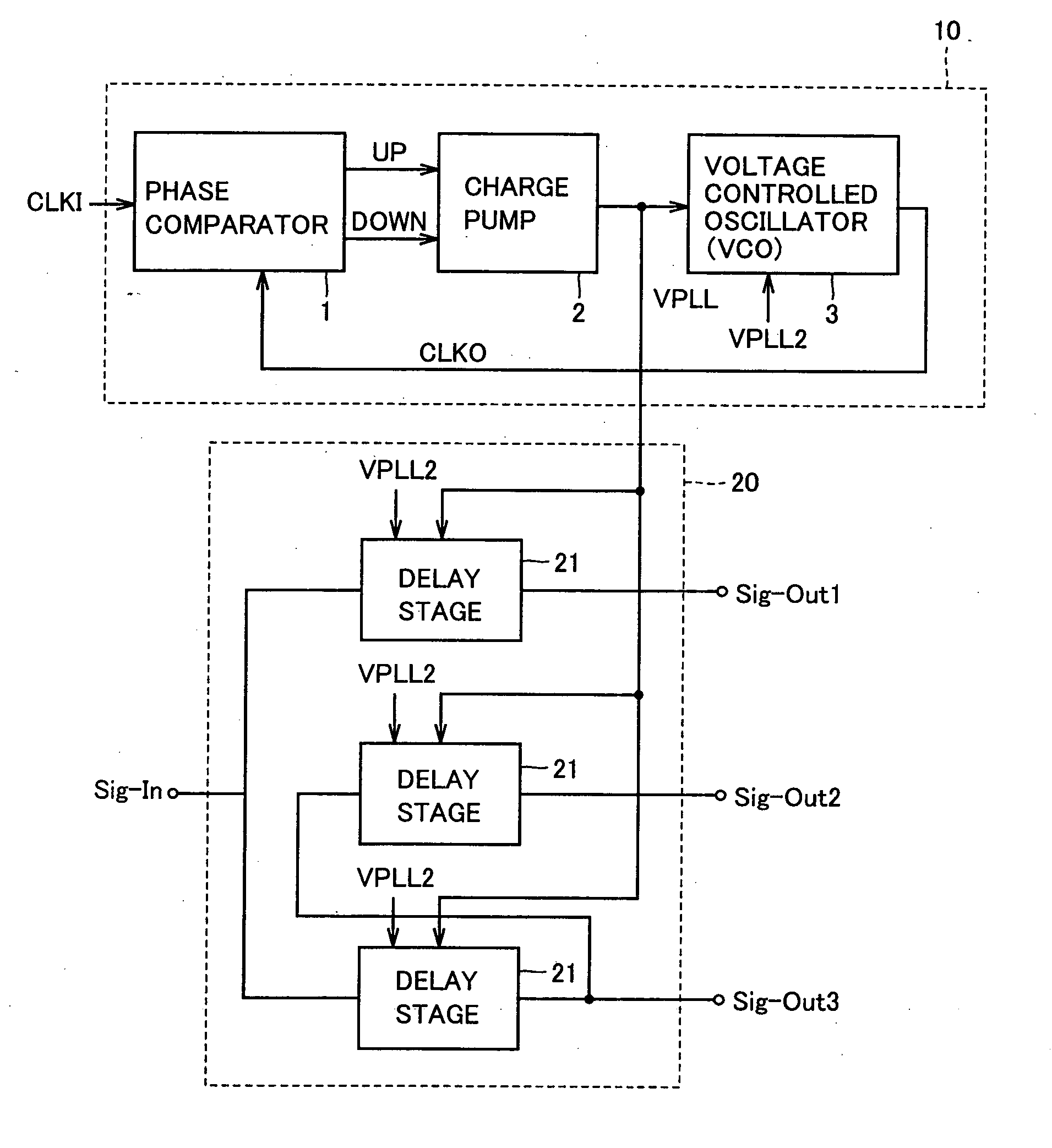
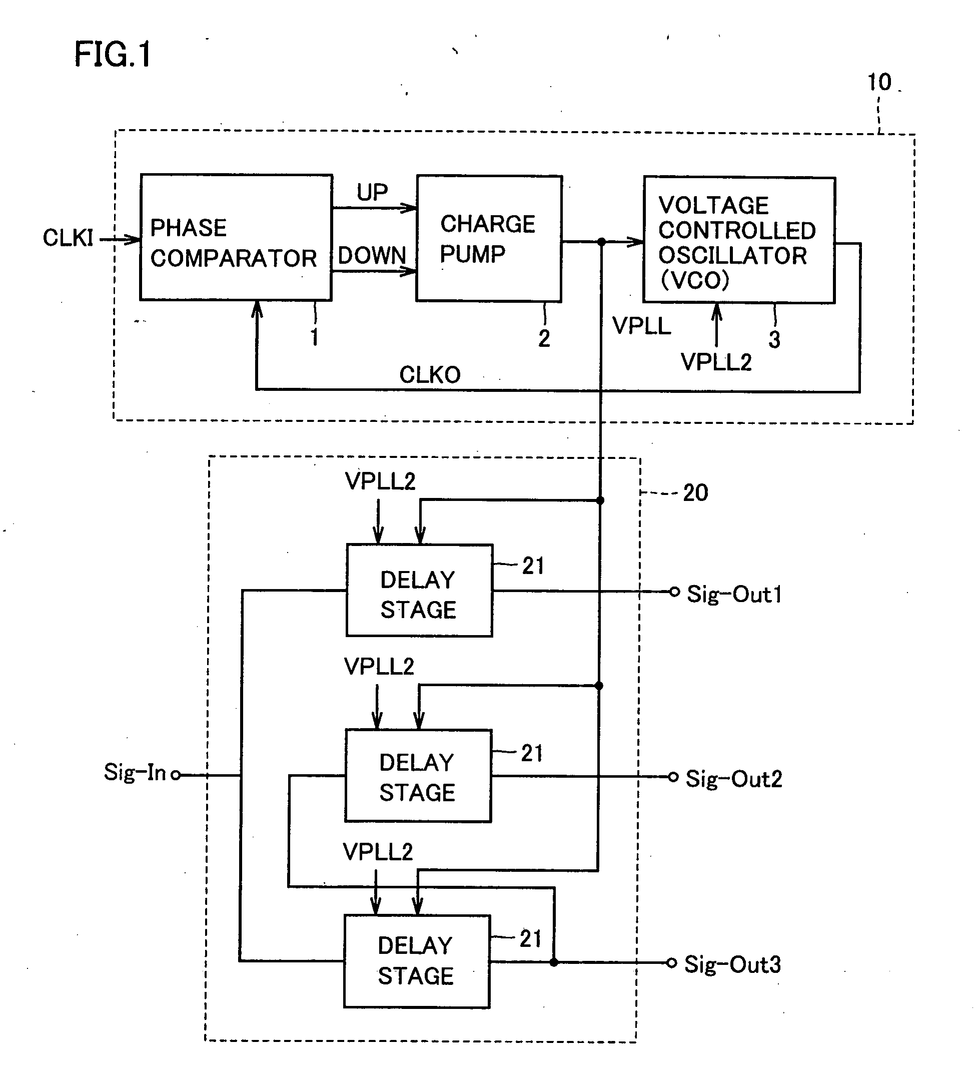
[0029]FIG. 1 is a schematic block diagram showing a configuration of a delay circuit according to a first embodiment of the present invention.

[0030] Referring to FIG. 1, the delay circuit includes a phase locked loop circuit 10 as a clock generating circuit for synchronizing an output clock CLKO with an input clock CLKI to output a control voltage VPLL of voltage controlled oscillator (VCO), and a delay section 20 of which delay time is controlled in response to the supply of control voltage VPLL.

[0031] Phase lock loop circuit 10 includes a phase comparator 1 comparing the phase of input clock CLKI and that of output clock CLKO, a charge pump circuit 2 providing control voltage VPLL in accordance with the result of phase comparison performed by phase comparator 1, and voltage controlled oscillator 3 generating output clock CLKO having the oscillation frequency in accordance with control voltage VPLL.

[0032] Further, output clock CLKO is supplied to an internal circuit (not shown) ...

second embodiment

[0082]FIG. 6 shows a schematic block diagram of the configuration of a delay circuit according to a second embodiment of the present invention.

[0083] Referring to FIG. 6, the delay circuit is formed of phase locked loop circuit 10 and a delay section 30. As for phase locked loop circuit10, since its configuration is similar to that of the delay circuit in the first embodiment shown in FIG. 1, only charge pump circuit 2 is illustrated and the detailed description will not be repeated.

[0084] Delay section 30 includes, as in the first embodiment, a plurality of delay stages 21. In FIG. 6, for simplifying the illustration, only one delay stage is illustrated and the rest of the delay stages are not shown. Delay stage 21 changes the delay time in accordance with a control signal based on control voltage VPLL of charge pump circuit 2, as in the first embodiment.

[0085] Delay section 30 further includes P-channel MOS transistors P2, P3, N-channel MOS transistors N2, N3, and an operationa...


PUM


Abstract

In a phase locked loop circuit, a phase comparator compares the phase of input clock and that of output clock, and provides a control signal as the comparison result. A charge pump circuit includes a clamp circuit, and based on the control signal, provides a control voltage of which lower limit is the reference voltage level. A voltage controlled oscillator receives the control voltage and a second control voltage from the outside and generates output clock having a frequency in accordance with the control voltages. Each delay stage of a delay section is configured with a plurality of delay units identical to that in the voltage controlled oscillator. The delay stage controls the delay time in response to the supply of the control voltage and the second control voltage.

Description

BACKGROUND OF THE INVENTION [0001] 1. Field of the Invention [0002] The present invention relates to a delay circuit delaying an input signal, and specifically, to a delay circuit with a timing adjustment function. [0003] 2. Description of the Background Art [0004] A general configuration of a delay circuit delaying an input signal is to employ a plurality of delay elements connected in series. For example, an inverter formed of a P-channel MOS transistor and an N-channel MOS transistor connected in series is generally used as a delay element in a semiconductor device of CMOS (Complementary Metal-Oxide Semiconductor device) structure. An input signal can be delayed for a desired delay time by selecting the number of stages of the delay elements in the delay circuit. [0005] On the other hand, it is difficult to render the characteristics of the elements forming the delay element uniform due to variations in a manufacturing process or fluctuations in the supply voltage or the ambient ...

Claims


Application Information

Patent Timeline
Patent Type & Authority Applications(United States)
IPC IPC(8): G06F1/06H03D3/24H03H11/26H03K5/13H03L7/00H03L7/081H03L7/089H03L7/099
CPCH03L7/0805H03L7/0995H03L7/0891H03L7/0812
Inventor DOSAKA, KATSUMI
Owner RENESAS ELECTRONICS CORP
Why Eureka
Try Eureka