Field emission type backlight device

a backlight device and field emission technology, applied in the field of field emission type backlight devices, can solve the problems of non-uniform emission, differences in input voltage and delay of signal pulse, luminance difference between beginning and end portions of signal voltage lines, etc., to achieve the effect of reducing power consumption and improving luminance uniformity

Inactive Publication Date: 2005-08-18
SAMSUNG SDI CO LTD
View PDF2 Cites 20 Cited by
  • Summary
  • Abstract
  • Description
  • Claims
  • Application Information

AI Technical Summary

Benefits of technology

[0013] The present invention provides a field emission type backlight devic

Problems solved by technology

Also, non-uniform emission tends to occur due to concentration of electric field in the edge of the cathode electrode 12.
This can lead to differences in input voltage and delay in sig

Method used


Image

  • Field emission type backlight device
  • Field emission type backlight device
  • Field emission type backlight device

Examples


Embodiment Construction

[0025] Exemplary embodiments of a field emission type backlight device of the present invention will now be described in detail with reference to the accompanying drawings.

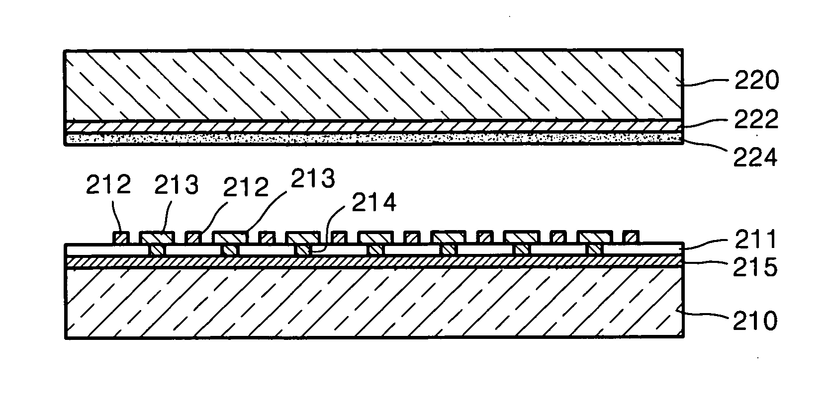
[0026] As shown in FIGS. 3A and 3B, upper and lower substrates 120 and 10 may be disposed facing each other with a gap between them. The upper and lower substrates 120 and 110 may be made of a transparent substrate such as glass substrate.

[0027] An anode electrode 122 may be provided on a lower side of the upper substrate 120. A fluorescent layer 124 may be provided on a lower side of the anode electrode 122. The anode electrode 122 may be provided on the entire surface of the upper substrate 120 and the fluorescent layer 124 may be provided on the entire surface of the anode electrode 122.

[0028] A lower gate electrode 115 may be provided on an upper side of the lower substrate 110, and an insulating layer 111 may be provided on an upper side of the lower gate electrode 115. A cathode electrode 112 and a plural...


PUM


Abstract

A field emission type backlight device can include upper and lower substrates facing each other with a gap between them, an anode electrode on a lower side of the upper substrate, a fluorescent layer on a lower side of the anode electrode, a lower gate electrode on an upper side of the lower substrate, an insulating layer on an upper side of the lower gate electrode, a cathode electrode on an upper side of the insulating layer, and a gate electrode that is provided on an upper side of the insulating layer and electrically connected to the lower gate electrode.

Description

BACKGROUND OF THE INVENTION [0001] This application claims priority to Korean Patent Application No. 10-2004-0006949, filed on Feb. 3, 2004, which is incorporated herein in its entirety by reference. [0002] 1. Field of the Invention [0003] The present invention relates to a field emission type backlight device. More particularly, it relates to a field emission type backlight device capable that may have improved luminance uniformity and reduced power consumption. [0004] 2. Description of the Related Art [0005] Liquid crystal displays (LCDs) often require a backlight device. A cold cathode fluorescent lamp (CCFL) has been commonly used as a line light source, and a light emitting diode (LED) as a point light source. More recently, field emission devices are being explored as alternative light sources. A field emission type backlight device has low power consumption and a relatively uniform luminance even in a wide area of light emission. [0006]FIG. 1A is a sectional view showing a co...

Claims


Application Information

Patent Timeline
IPC IPC(8): G02F1/13357H01J3/02H01J63/06
CPCB82Y10/00G02F1/133602H01J2201/30469H01J63/06H01J3/022E03F5/0404E03F5/06E03F5/14E03F3/046E03F2005/0415
Inventor OH, TAE-SIKKIM, JONG-MINJUNG, JAE-EUNKIM, JUNG-WOOLEE, HANG-WOO
Owner SAMSUNG SDI CO LTD
Why Eureka
Try Eureka