Implementation of MOS capacitor in CT scanner data acquisition system

a mos capacitor and data acquisition technology, applied in the field of circuitry for ct (computed tomography) scanner data acquisition system, can solve the problems of increasing the cost of making a high-resolution ct scanner system, unable to significantly reduce the amount of chip area required to implement the prior art ct scanner data acquisition circuitry without unacceptably increasing the amount of noise generated, and it is impractical to provide a large number of front-end integrators in a

Inactive Publication Date: 2005-08-18
TEXAS INSTR INC
View PDF11 Cites 26 Cited by
  • Summary
  • Abstract
  • Description
  • Claims
  • Application Information

AI Technical Summary

Benefits of technology

[0013] Accordingly, it is an object of the invention to provide an improved CT scanner data acquisition circuit that greatly reduc

Problems solved by technology

Although the low variation in the capacitance of a poly capacitor is very desirable, the very large physical size of a large value poly compensation capacitor Cc greatly limits the number of the front-end integrators that can be provided on a practical integrated circuit chip of economic size, and therefore greatly increases the cost of making a high-resolution CT scanner system having, for example, thousands of photodiode detectors.
Furthermore, the am

Method used


Image

  • Implementation of MOS capacitor in CT scanner data acquisition system
  • Implementation of MOS capacitor in CT scanner data acquisition system
  • Implementation of MOS capacitor in CT scanner data acquisition system

Examples


Embodiment Construction

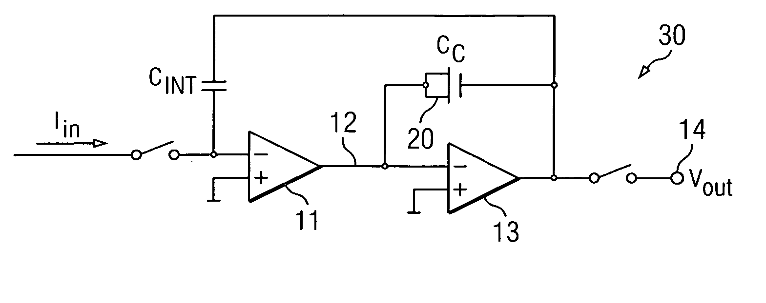
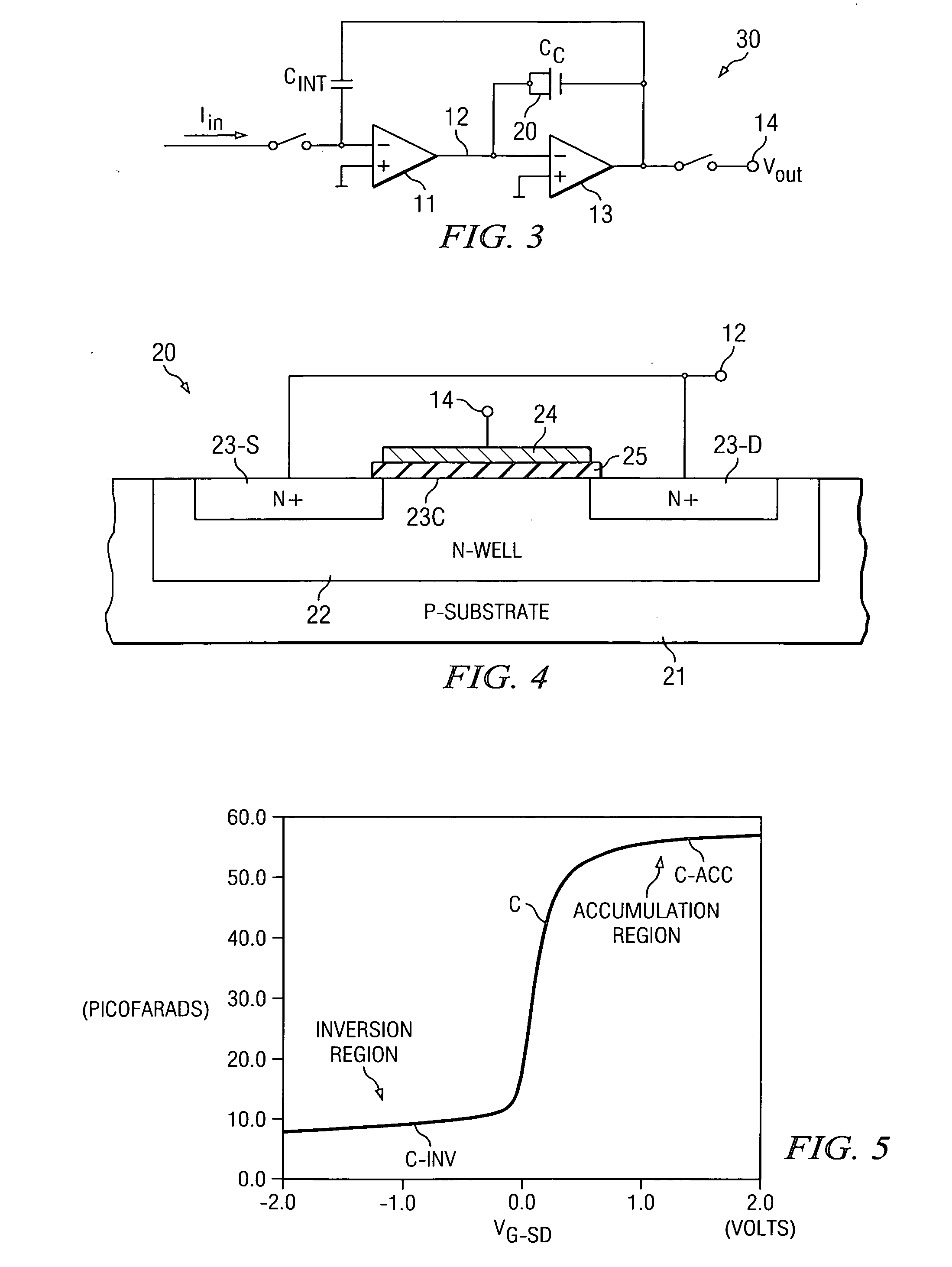
[0028]FIG. 3 shows an improved front-end integrator 30 which may be substituted for prior art front-end integrators 2A-1, 2A-2, 2B-1 and 2B-2 in the two-channel data acquisition system of FIG. 2. The only difference between the structure of front-end integrator 30 of FIG. 3 and front-end integrator 2A-1 of FIG. 2 is that in improved front-end integrator 30 the poly compensation capacitor Cc of FIG. 2 has been replaced by an N-channel MOS compensation capacitor 20, also referred to as MOS compensation capacitor Cc, the capacitance of which is also indicated by the symbol Cc. (A P-channel MOS compensation capacitor also might be usable in some cases.) The switches ensure that only one integrator is connected to input current Iin and the delta-sigma ADC at a time.

[0029]FIG. 4 shows a section view which shows the structure of N-channel MOS compensation capacitor 20. MOS compensation capacitor 20 as shown in FIG. 4a includes an N-channel “well” region 22 formed in a P-type substrate 21....


PUM


Abstract

An integrator circuit includes an input conductor for conducting an input current, a first amplifier stage having a first input coupled to the input conductor and a second input coupled to receive a reference voltage and a second amplifier stage having a output and an input coupled to an output of the first amplifier stage. An integrating capacitor is coupled between the first input of the first amplifier stage and the output of the second amplifier stage, and a compensation capacitor comprised of an MOS capacitor is coupled between the input and the output of the second amplifier stage. The integrator circuit is especially adapted for use in a CT scanner data acquisition system.

Description

BACKGROUND OF THE INVENTION [0001] The present invention relates generally to circuitry for CT (computed tomography) scanner data acquisition systems, and more particularly, the present invention relates to circuitry improvements that make it possible to provide a large number of input channels on a single integrated circuit that includes multiple front-end integrators each coupled to receive an input current produced by a corresponding photosensor such as a photodiode receiving light produced by a scintillator in response to x-rays. [0002] A typical CT scanner data acquisition system includes, for each photodiode of a photodiode array, a corresponding front-end integrator that converts the output current of the photodiode to a corresponding output voltage and holds that voltage during sampling thereof by means of a sample / hold circuit. The CT scanner data acquisition system also includes high-resolution ADCs (analog-to-digital converters). A scintillator is typically placed in fron...

Claims


Application Information

Patent Timeline
IPC IPC(8): A61B6/03G06G7/186G11C27/02H03K5/00H03K17/00H03K19/094H03K19/20
CPCG06G7/186A61B6/032H04N5/32
Inventor ZHOU, BINLINGTODSEN, JAMES L.
Owner TEXAS INSTR INC
Why Eureka
Try Eureka