High frequency switch circuit

a high-frequency switch and circuit technology, applied in electronic switching, pulse automatic control, pulse technique, etc., can solve the problems of increasing the chip area reducing the handling power, and increasing the size of the high-frequency switch circuit constructed as an integrated circuit, so as to increase the handling power and reduce the control potential of the fet in an off-state state. , the effect of increasing the handling power

Inactive Publication Date: 2005-08-18
NEC CORP
View PDF5 Cites 46 Cited by
  • Summary
  • Abstract
  • Description
  • Claims
  • Application Information

AI Technical Summary

Benefits of technology

[0011] A high-frequency switch circuit according to the present invention includes a plurality of high-frequency switch means for passing and blocking a high-frequency signal between an input terminal and an output terminal depending on a control potential applied as a control signal, detecting means for detecting the high-frequency signal which passes through the high-frequency switch means, and a control potential generating circuit for changing the control potential applied to at least one of the plurality of high-frequency switch means in order to increase the difference between the control potential applied to the high-frequency switch means which is in an ON-state and the control potential applied to the high-frequency switch means which is in an OFF-state, depending on the amplitude of the high-frequency signal detected by the detecting means.
[0016] According to the first and second aspects described above of the present invention, the gate potential of the FET in the ON-state side or the OFF-state side is increased or lowered to increase VH−VL in equation (1), thereby increasing the handling power. Therefore, a high-frequency switch circuit may be constructed to incorporate both the arrangements according to the first and second aspects.
[0017] According to the present invention, the control potential generating circuit increases the difference between the control potential applied to the high-frequency switch means which is in an ON-state and the control potential applied to the high-frequency switch means which is in an OFF-state, as the input amplitude of the high-frequency signal detected by the high-frequency switch means increases. According to the present invention, therefore, VH−VL indicated in the equation (1) increases, and the handling power can be increased without increasing the number n of FETs connected in cascade. The high-frequency switch circuit does not require control signals from an external circuit except for control potential signals of switches, ie., switching signals.
[0018] According to the first aspect of the invention, the control potential generating circuit automatically makes the magnitude of an increase in the potential greater when the high-frequency switch means is in an ON-state and makes the magnitude of an increase in the potential smaller when the high-frequency switch means is in an OFF-state, depending on the ON-state and the OFF-state of the high-frequency switch means. Therefore, it is not necessary to control the increase in the control potential. Similarly, according to the second aspect of the invention, the control potential generating circuit automatically makes the magnitude of a reduction in the potential greater when the high-frequency switch means is in an OFF-state and makes the magnitude of a reduction in the potential smaller when the high-frequency switch means is in an ON-state, depending on the ON-state and the OFF-state of the high-frequency switch means. Consequently, it is not necessary to control the reduction in the control potential.
[0019] According to the present invention, therefore, even if a control potential is low, a high-frequency switch circuit having a high handling power capability can be realized in a small chip area.

Problems solved by technology

When the high-level control potential of the switch becomes lower, VH in equation (1) becomes lower, resulting in a reduction in the handling power.
The high-frequency switch circuit with a plurality of cascaded FETs is disadvantageous in that as the control potential is lowered, the handling power is lowered, and that if the handling power is to be increased, then the number of cascaded FETs is increased, resulting in an increase in the size of the high-frequency switch circuit constructed as an integrated circuit.
The high-frequency switch circuit as disclosed in JP-A-10-084267 is problematic in that in order to make a selection as to whether the DC potential generated from the high-frequency signal is to be applied to the gate of the FET or not, the FET for high-frequency switching and a selector circuit, i.e., the switch circuit and a power supply and a control signal for controlling the switch circuit, are required, with the result that the chip area of the high-frequency switch circuit constructed as an integrated circuit tends to increase.

Method used


Image

  • High frequency switch circuit
  • High frequency switch circuit
  • High frequency switch circuit

Examples


first embodiment

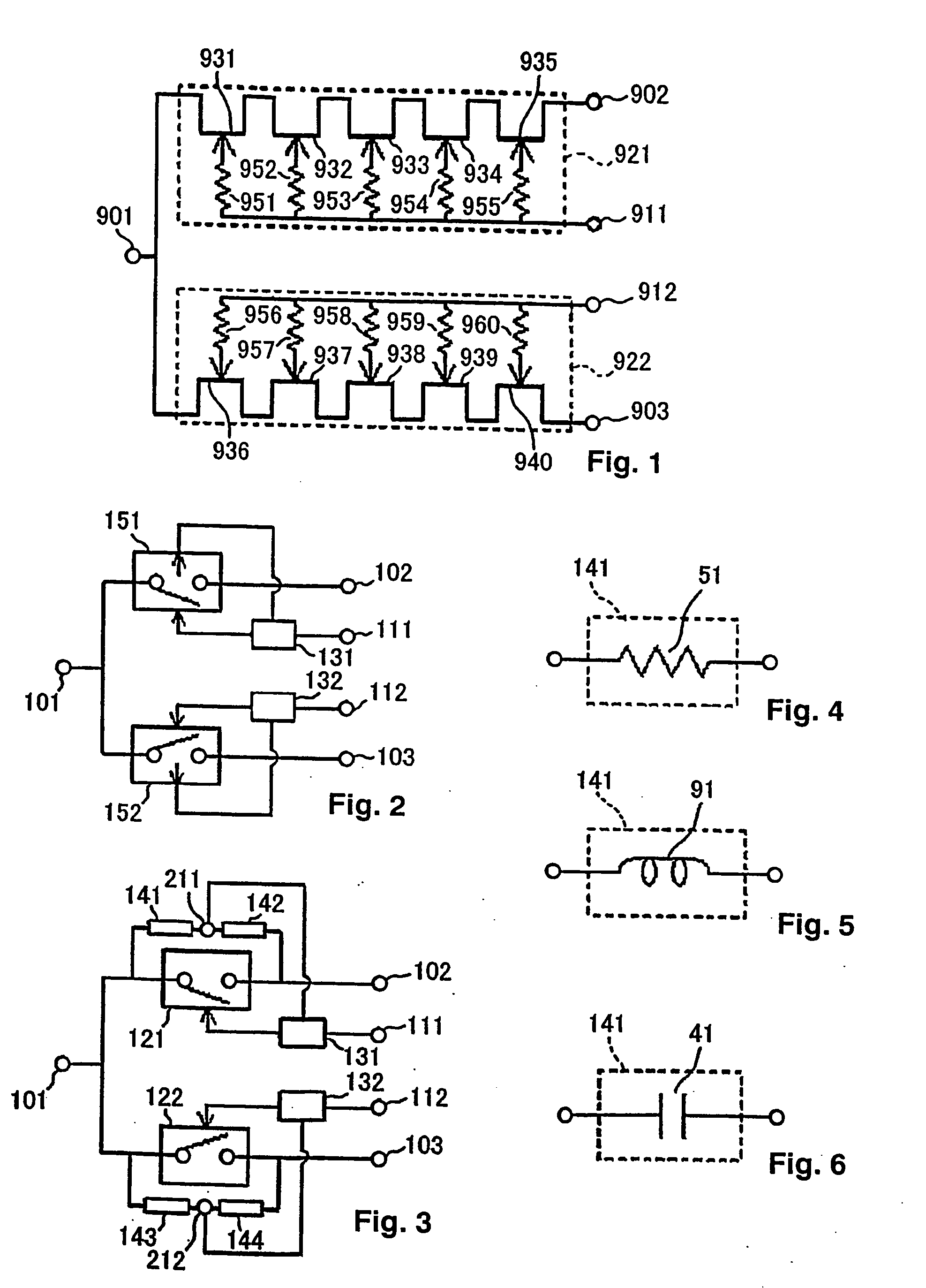
[0050]FIG. 2 is a block diagram showing a schematic arrangement of a high-frequency switch circuit according to the present invention.

[0051] The high-frequency switch circuit shown in FIG. 2 is suitable for being arranged as a semiconductor integrated circuit, and is configured as an SPDT circuit. The high-frequency switch circuit has high-frequency terminal 101 as a common terminal, first high-frequency circuit section 151 having an input terminal connected to high-frequency terminal 101, high-frequency terminal 102 connected to an output terminal of first high-frequency circuit section 151, second high-frequency circuit section 152 having an input terminal connected to high-frequency terminal 101, high-frequency terminal 103 connected to an output terminal of second high-frequency circuit section 152, first and second control potential input terminals 111, 112 for being supplied with a pair of complementary control potentials, i.e., control signals, first voltage boosting circuit ...

fourth embodiment

[0080]FIG. 23 shows a specific circuit arrangement of the high-frequency switch circuit according to the FETs 1, 2 connected in cascade and resistive elements 61, 62 connected to the respective gates of FETs 1, 2 make up high-frequency switch 121. Similarly, FETs 3, 4 and resistive elements 63, 64 make up high-frequency switch 122. FETs 5, 6 and resistive elements 65, 66 make up high-frequency switch 123, and FETs 7, 8 and resistive elements 67, 68 make up high-frequency switch 124. Voltage boosting circuits 131, 133 employ the arrangement shown in FIG. 13.

[0081] Operation of the high-frequency switch circuit according to the fourth embodiment will be described below.

[0082] Referring again to FIG. 22, control potentials having binary levels, i.e., high and low levels, are complementarily applied as control signals to control potential input terminals 111, 112. It is assumed that a high-level potential is applied to control potential input terminal 111 and a low-level potential is ...

fifth embodiment

[0088]FIGS. 25 and 26 show specific circuit arrangements of the high-frequency switch circuit according to the The high-frequency switch circuit shown in FIG. 25 is equivalent to the high-frequency switch circuit shown in FIG. 23 except that the high-frequency detecting terminals of voltage boosting circuits 131, 132 are connected respectively to high-frequency terminals 102, 103. The high-frequency switch circuit shown in FIG. 26 is similar to the high-frequency switch circuit shown in FIG. 25 except that resistive element 58 is inserted between capacitive element 43 and the high-frequency detecting terminal of each of voltage boosting circuits 131, 132.

[0089] Operation of the high-frequency switch circuit according to the fifth embodiment will be described below.

[0090] Referring again to FIG. 24, control potentials having binary levels, i.e., high and low levels, are complementarily applied as control signals to control potential input terminals 111, 112. It is assumed that a hi...


PUM


Abstract

A high-frequency switch circuit has a plurality of high-frequency switches for passing and blocking a high-frequency signal between an input terminal and an output terminal depending on a control potential applied as a control signal, a high-frequency detecting terminal for detecting high-frequency signal passing through the high-frequency switch which is in ON-state, and a voltage boosting circuit for generating a potential for increasing the control potential applied to the high-frequency switch which is in ON-state in order to increase difference between the control potential applied to the high-frequency switch which is in an ON-state and the control potential applied to the high-frequency switch which is in an OFF-state, depending on an intensity or amplitude of the detected high-frequency signal.

Description

TECHNICAL FIELD [0001] The present invention relates to a high-frequency switch circuit, and more particularly to a high-frequency switch circuit which is of a small size and is capable of switching between high electric power levels. BACKGROUND ART [0002] Known high-frequency switch circuits that are controlled by control potentials which are input as control signals employ field-effect transistors (FETs) or diodes. For example, Japanese Patent Laid-open Application No. 8-139014 (JP-A-08-139014) discloses a high-frequency switch circuit having a SPDT (Single-Pole, Double-Throw) structure which is made up of a plurality of cascaded FETs integrated on a GaAs substrate, as a semiconductor integrated circuit (IC). [0003]FIG. 1 shows such a conventional SPDT circuit by way of example. The high-frequency switch circuit shown in FIG. 1 has three high-frequency terminals 901 to 903 and two control potential input terminals 911, 912 for being supplied with control potentials as control sign...

Claims


Application Information

Patent Timeline
Patent Type & Authority Applications(United States)
IPC IPC(8): H03K17/693H03K17/06H04B1/48
CPCH03K17/063H04B1/48H03K17/693
Inventor TAKAHASHI, YUJINUMATA, KEIICHI
Owner NEC CORP
Why Eureka
Try Eureka