Display device, drive method thereof, and drive system thereof

a technology of a display device and a drive method, applied in the field of display devices, can solve the problems that the power reduction of conventional devices attempted to achieve is not sufficient, and achieve the effect of reducing electric power consumption

Active Publication Date: 2005-08-18
SHARP KK
View PDF10 Cites 21 Cited by
  • Summary
  • Abstract
  • Description
  • Claims
  • Application Information

AI Technical Summary

Benefits of technology

[0015] It is an object of the present invention to provide a liquid crystal display device capable of...

Problems solved by technology

However, measures for reducing power consumption attempted in the...

Method used


Image

  • Display device, drive method thereof, and drive system thereof
  • Display device, drive method thereof, and drive system thereof
  • Display device, drive method thereof, and drive system thereof

Examples


first embodiment

[0037] One embodiment of the present invention will be described below based on the accompanying drawings.

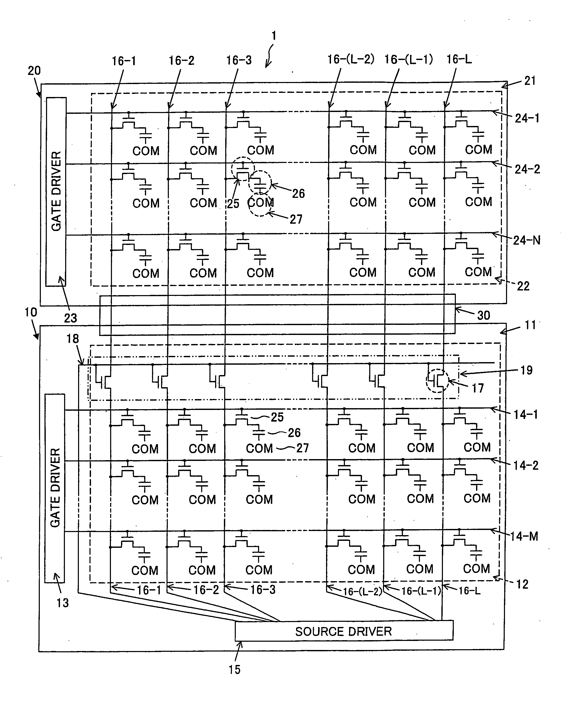
[0038]FIG. 1 is a circuit diagram showing a liquid crystal display device (display device) 1 of the present embodiment. As shown in FIG. 1, the liquid crystal display device 1 is a twin-panel display device which has a first liquid crystal panel (first display means) 10 and a second liquid crystal panel (second display means) 20.

[0039] The first liquid crystal panel 10 includes a TFT substrate 11, which is provided with a thin film transistor (TFT) 25; a counter substrate 12, which faces the TFT substrate 11; and a liquid crystal layer, which serves as a display medium sandwiched between the TFT substrate 11 and the counter substrate 12. The liquid crystal layer constitutes a liquid crystal capacitor 26.

[0040] Provided on the TFT substrate 11 are a plurality of gate bus lines (gate signal lines) 14 and a plurality of source bus lines (source signal lines) 16. Provided near a ...

second embodiment

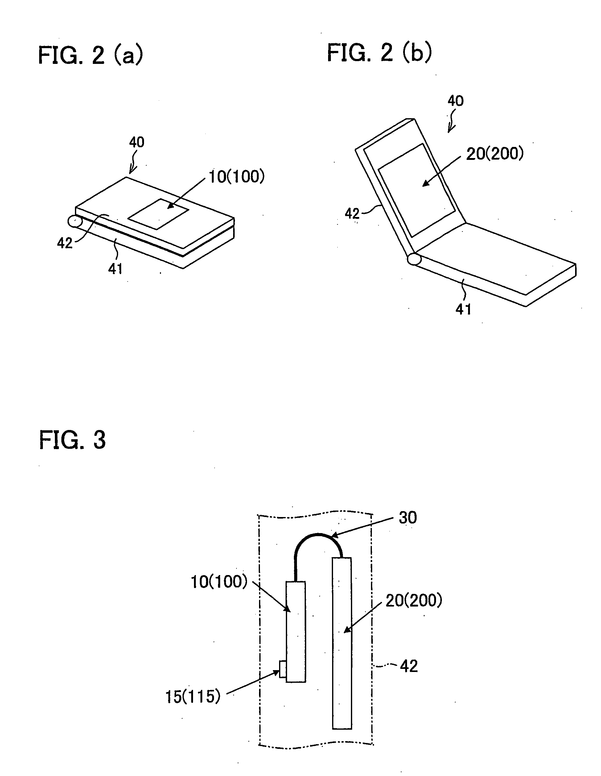
[0065] Another embodiment of the present invention will be described below based on the accompanying drawings. As shown in FIG. 6, a liquid crystal display device (display device) 2 of the present embodiment is a twin-panel display device which is constituted of a sub panel (first display means) 100 and a main panel (second display means) 200. The sub panel 100 and the main panel 200 are active matrix panels. A gate bus line of the sub panel 100 and a gate bus line of the main panel 200 are provided with and driven by gate drivers 113 and 123 respectively. A source bus line of the sub panel 100 and a source bus line of the main panel 200 are provided with and driven by one source driver 115 for common use in the sub panel 100 and the main panel 200.

[0066] The source driver 115 outputs a display data signal, which is then supplied to the source bus line of the main panel 200 through the source bus line of the sub panel 100. Furthermore, the source bus line of the sub panel 100 and t...


PUM


Abstract

The sub panel 100, having a plurality of gate bus lines 14, source bus lines 16, TFTs 25 and pixel electrodes, is provided with a source driver 15. The main panel 200 has a plurality of gate bus lines 24, source bus lines 16, TFTs 25 and pixel electrodes, each of the source bus lines 16 being connected to the corresponding source bus lines 16 of the first liquid crystal panel 10 through a switching TFT 17. The main panel 200, sharing the source driver 15 with the first liquid crystal panel 10, is less frequently used for display than the first liquid crystal panel 10, and is disconnected by the switching TFT 17 when only the sub panel 100 is used. This makes it possible to device a twin-panel display device low in electric power consumption.

Description

[0001] This Nonprovisional application claims priority under 35 U.S.C. § 119(a) on Patent Application No. 040494 / 2004 filed in Japan on Feb. 17, 2004, the entire contents of which are hereby incorporated by reference. FIELD OF THE INVENTION [0002] The present invention relates to a display device of a liquid crystal display apparatus and the like including a plurality of active matrix display panels. The present invention also relates to a drive method of the display device. BACKGROUND OF THE INVENTION [0003] Recently, a so-called twin panel formed of two display panels has been heavily used in a portable device etc., particularly in a foldable mobile phone. FIG. 11 is a circuit diagram showing a twin panel 581 as an example of such a twin panel. The twin panel 581 is formed of a main panel 582 and a sub panel 583. [0004] The main panel 582 includes a TFT substrate 584, which has a substrate and a thin film transistor (TFT) 592 provided thereon; a counter substrate 585, which faces ...

Claims


Application Information

Patent Timeline
IPC IPC(8): G02F1/1333G02F1/133G02F1/1343G02F1/1368G09F9/35G09F9/40G09G3/20G09G3/36
CPCG09G3/3688G09G3/3666G02F1/133
Inventor TANAKA, NORIYUKIKUMADA, KOUJI
Owner SHARP KK
Why Eureka
Try Eureka