Large cavity wafer-level package for MEMS

a technology of mems and wafers, applied in the direction of instruments, optical elements, forming microstructural systems, etc., can solve the problems of affecting the performance of the device, affecting the operation of the device, and the application in which electrically conductive surfaces are required on optically transparent windows. are particularly challenging, and many mems devices do not have a sufficient height for movable and actuable devices

Inactive Publication Date: 2005-08-25
NANOGEAR
View PDF19 Cites 90 Cited by
  • Summary
  • Abstract
  • Description
  • Claims
  • Application Information

AI Technical Summary

Problems solved by technology

With optical systems, hermetic sealing is particularly critical to the long-term stability of active optical components, which can be affected by humidity and other environmental factors that can degrade device performance.
Micromirrors and other moving components of MEMS or micro-optical-electromechanical systems (MOEMS) generally impose further constraints to package designs, such as requiring electrostatic discharge protection.
Applications in which electrically conductive surfaces are required on optically transparent windows are particularly challenging since most conductive materials are opaque.
While packages have been designed to provide electrostatic isolation, not many have a sufficient height for movable and actuatable MEMS devices, as pointed out in “Resiliently Packaged MEMS Device and Method for Making Same,” Jin et al., U.S. Patent Application No. 2002 / 0097952 published Jul. 25, 2002.
For example, some adhesives and polymers cannot be used in MEMS packages because they are neither conductive nor hermetic.
The glass alone does not provide a conductive package to prevent electrostatic discharge.
Bonding by thermocompression requires heating the package to high temperatures that may damage the MEMS or other on-chip devices.
Bonding with adhesives and polymers is limited in their abilities to provide a hermetic and conductive package.
While the packages and packaging methods described above have heretofore produced packages for micro-devices, the relatively high cost of manufacturing is a significant obstacle to their widespread application.
Many of the aforementioned integrated packages have insufficient height to accommodate movable MEMS devices such as actuated micromirrors in an optical MEMS switch.

Method used


Image

  • Large cavity wafer-level package for MEMS
  • Large cavity wafer-level package for MEMS
  • Large cavity wafer-level package for MEMS

Examples


Embodiment Construction

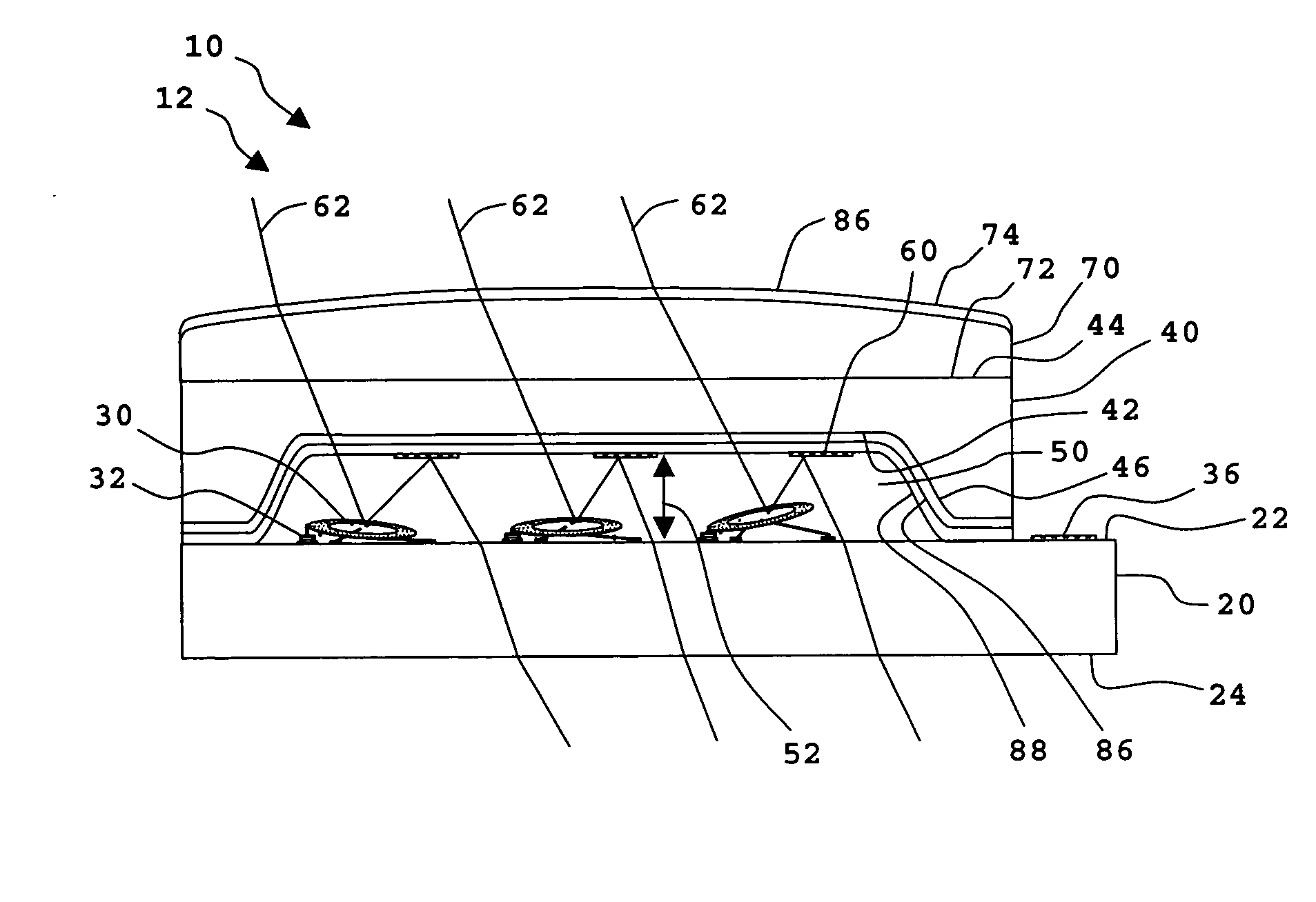
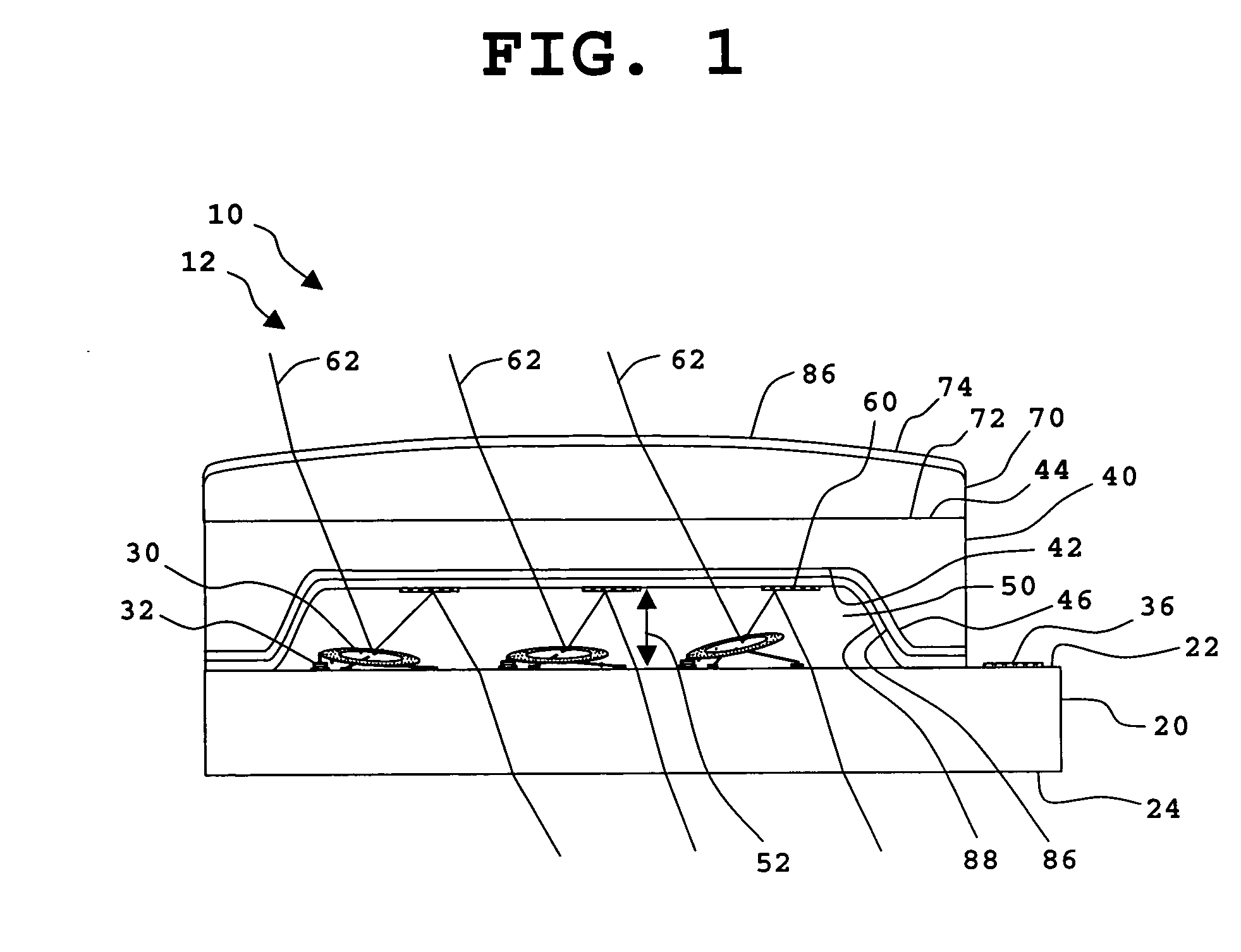
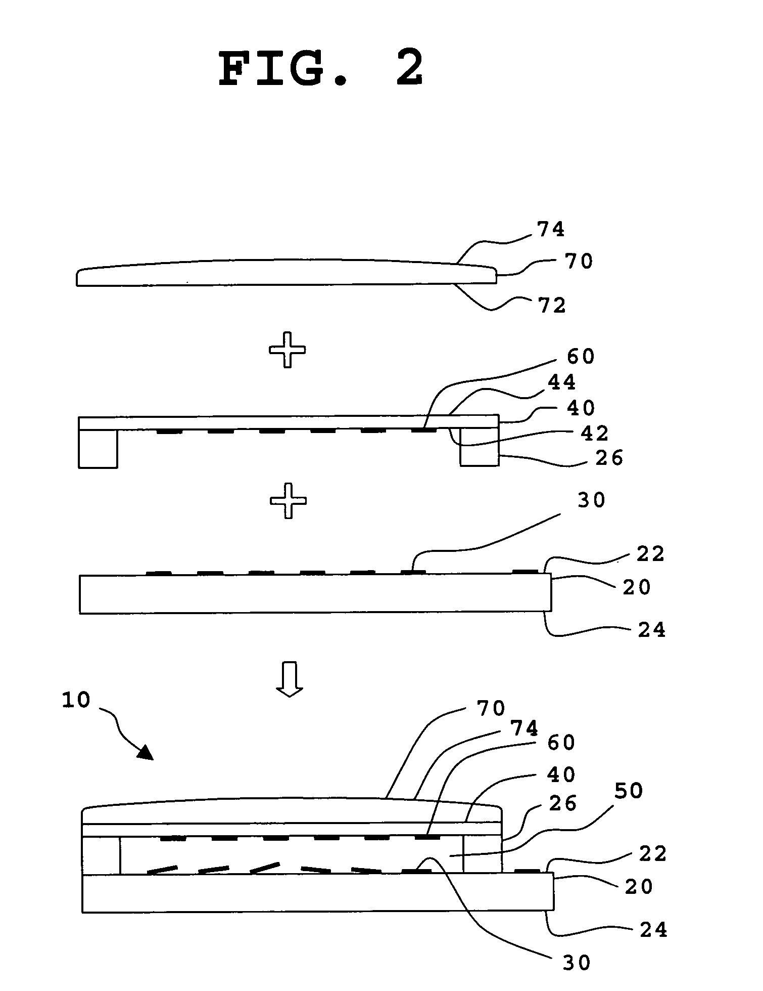
[0029]FIG. 1 illustrates a cross-sectional view of a packaged micromirror assembly, in accordance with one embodiment of the present invention. Packaged micromirror assembly 10 is diced or otherwise cut from a wafer-level package 12 for an array of actuatable micromirrors 30 or other devices. Packaged micromirror assembly 10 includes a substrate 20 having a substrate surface 22, a plurality of actuatable micromirrors 30 coupled to substrate surface 22, and an optical window 40 attached to substrate surface 22. Optical window 40 and substrate surface 22 cooperate to form one or more sealed cavities 50 between an inner surface 42 of optical window 40 and substrate surface 22. Inner surface 42 of optical window 40 faces sealed cavity 50, and may include additional layers such as an anti-reflective layer 86, a transparent conductive layer 88, or a combination thereof. Optical window 40, when attached to substrate surface 22, forms a lid or cap over actuatable micromirrors 30 or other de...


PUM


Abstract

The invention provides a wafer-level package for a micromirror array. The wafer-level package includes a substrate including a wafer having a substrate surface with a plurality of actuatable micromirrors coupled to the substrate surface. An optical window is attached to the substrate surface to form at least one sealed cavity between an inner surface of the optical window and the substrate surface. A beam of light transmitted through the optical window is redirected by at least one actuatable micromirror within the sealed cavity.

Description

FIELD OF THE INVENTION [0001] The present invention relates generally to optical switches and beam-steering devices, and more specifically to wafer-level packages with large cavities for MEMS micromirror arrays. BACKGROUND OF THE INVENTION [0002] Photonic, optical and micromechanical devices are typically packaged so that active elements such as micromirrors are disposed within a sealed chamber to protect them from handling, mechanical, environmental, or other damage. Existing packaging systems for microelectromechanical systems (MEMS) devices, which are based on commercially available military hybrid packages and multi-layer ceramic packages, include hermetically sealed chambers to prevent the influx, egress or exchange of gases, moisture and particulates between the chamber and the environment. With optical systems, hermetic sealing is particularly critical to the long-term stability of active optical components, which can be affected by humidity and other environmental factors th...

Claims


Application Information

Patent Timeline
Patent Type & Authority Applications(United States)
IPC IPC(8): G02B26/08H01L33/00
CPCB81B2201/042B81C1/00214G02B26/0841B81C2203/0118G02B26/0833B81C1/00317
Inventor GUPTA, PAVAN O.HAGELIN, PAUL M.ANDRONACO, GREGORY
Owner NANOGEAR
Why Eureka
Try Eureka