Micromirror arrays having self aligned features

a technology of micromirror arrays and features, which is applied in the field of micromirror arrays having self-aligning features, can solve the problems of reducing the signal to noise ratio resulting from either or both of lower signals, and increasing the difficulty of multiplexing

Active Publication Date: 2011-09-15
PACIFIC BIOSCIENCES
View PDF16 Cites 65 Cited by
  • Summary
  • Abstract
  • Description
  • Claims
  • Application Information

AI Technical Summary

Benefits of technology

[0022]In some embodiments the alignment between the nanoscale aperture and the corresponding micromirror is better than for a micromirror array for which lateral dimensions of both the protrusions and the nanoscale apertures are not defined in a single patterning step. In some embodiments the alignment is 10 percent better over 100 micromirrors. In some embodiments the alignment is 20 percent better over 100 micromirrors.

Problems solved by technology

In optical analyses, increasing multiplex often poses increased difficulties, as it may require more complex optical systems, increased illumination or detection capabilities, and new reaction containment strategies.
In some cases, systems seek to increase multiplex by many fold, and even orders of magnitude, which further implicate these considerations.
Likewise, in certain cases, the analytical environment for which the systems are to be used is so highly sensitive that variations among different analyses in a given system may not be tolerable.
These goals are often at odds with a brute force approach of simply making systems bigger and of higher power, as such steps often give rise to even greater consequences, e.g., in inter reaction cross-talk, decreased signal to noise ratios resulting from either or both of lower signal and higher noise, and the like.

Method used


Image

  • Micromirror arrays having self aligned features
  • Micromirror arrays having self aligned features
  • Micromirror arrays having self aligned features

Examples


example 1

Micromirror Arrays

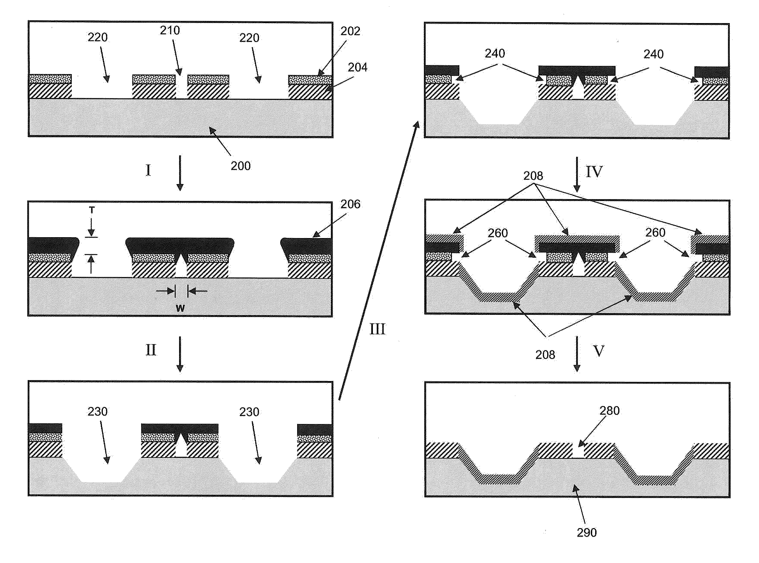
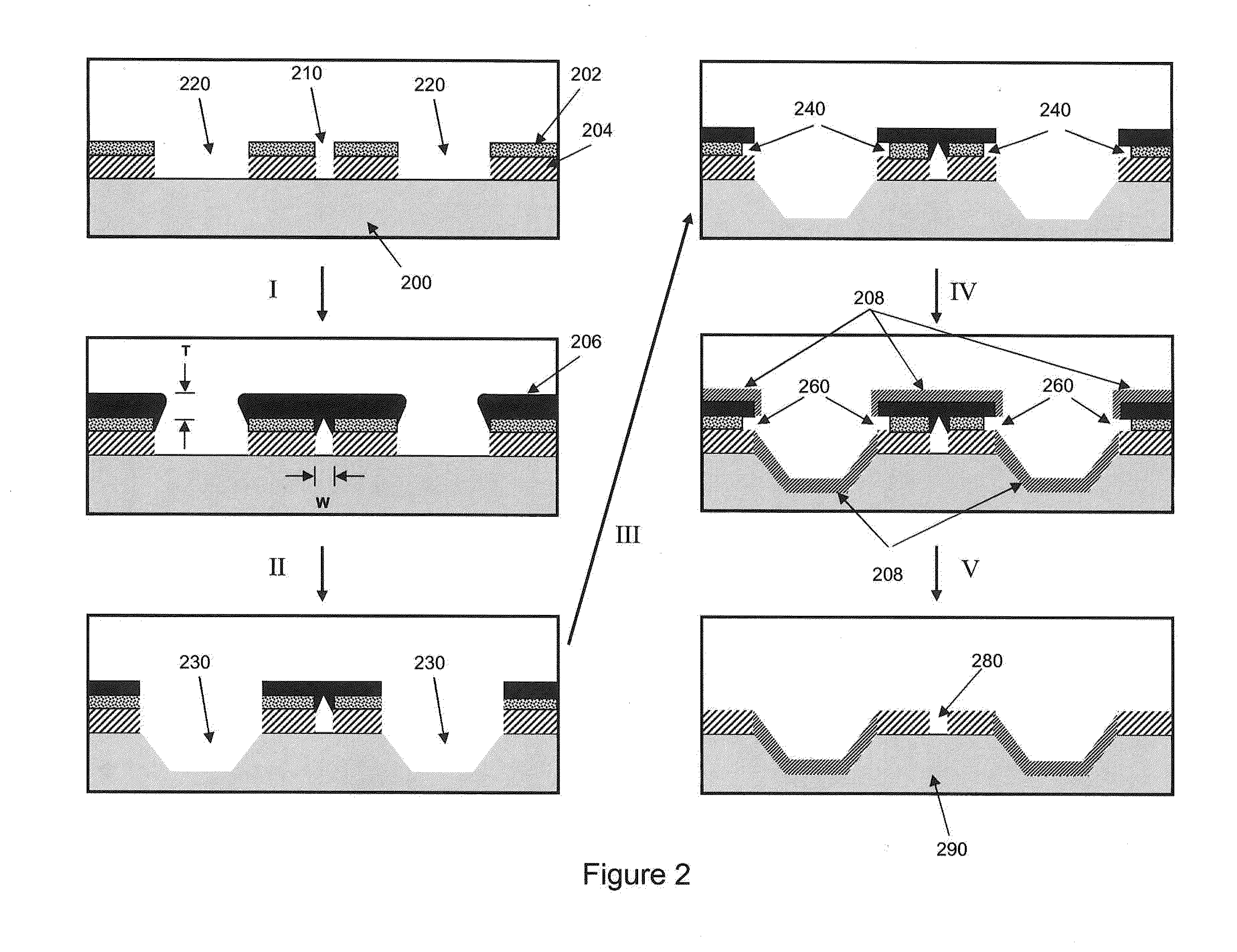
[0198]An array of micromirrors having nanoscale apertures on their tops was fabricated starting from a fused silica (FuSi) wafer using a process as described in FIG. 3A. First, 110 nm of aluminum was deposited at room temperature onto the FuSi. Onto the Fusi was deposited a 500 nm amorphous silicon hard-mask at 350° C., 0.9 Torr, and 60 W. The first lithography was done using a 490 nm thick photoresist in an asm1-PAS5500 DUV stepper. This step defined both the small features which will become the nanoscale apertures, and the large features which will define the micromirror protrusions. The hard mask was etched in a Centura platform using HBr=100 sccm, Cl2=60 sccm, RF=700 W, Bias=50 W, at 20 mTorr, followed by etching of the aluminum in the same system using Cl2=90 sccm, BCl3=45 sccm, RF=1000 W, Bias=100 W at 10 mTorr. The second, non-critical, lithography (step I) was done using 2 μm photoresist in the same stepper. Then the mirror was etched (step II) in Centura p...

example 2

Theoretical Modeling of Conical Mirror Substrates

[0202]Structures were modeled using the various components illustrated in FIGS. 18 and 19, respectively. For example, with respect to the straight conical structure illustrated in FIG. 18, dimensions were set as follows: d1=1.25 μm; d2=5 μm and h=4.69 μm. The model assumed that an objective lens used to collect emitted light from the substrate / reflector component has a numerical aperture of 0.5 with a highest collection angle of + / −20 degrees with respect to the optical axis, thereby providing a collection angle with respect to the bottom surface of the substrate of from 70 to 110 degrees. Based upon the conical model shown in FIG. 16, the ray angle that is reflected out of the cone is from 43.58 (⊖tr) to 105.52 (⊖br) degrees.

[0203]For the two staged conical reflector shown in FIG. 19, the dimensions were set to: d1=1.25 μm; d2=3 μm; d3=5 μm; h1=1 μm; and h2=3.69 μm. In this case, the ray angle that is reflected and comes out of the r...

example 3

Gain Measurements on Conical Micromirror Structures

[0205]Measurements were performed to determine the amount of gain that would be obtained from using micromirror structures coupled to zero mode waveguides. A substrate was prepared with FuSi having ZMW structures on the tops of micromirrors and having comparable ZMW structures on the planar portions of the substrate. FIG. 20 shows a schematic illustration of the experimental setup in which light is transmitted through the ZMW structures on the substrate. The light transmitted through the ZMW structures is collected with an optical train and detected on a CCD camera. The numerical aperture of the optical detection system was 0.5. Table 1 lists representative measurements of detected intensity from ZMW structures on the flat region of the substrate, and from ZMW structures on the tops of micromirror structures. The calculated gain from these measurements is about 5.9. It is understood that the measured gain will depend on the numeric ...


PUM

PropertyMeasurementUnit
thicknessaaaaaaaaaa
thicknessaaaaaaaaaa
thicknessaaaaaaaaaa

Abstract

Methods, arrays, and systems for the optical analysis of multiple chemical, biological, or biochemical reactions are provided. The invention includes methods for producing arrays of micromirrors on transparent substrates, each micromirror comprising a nanostructure or optical confinement on its top. The arrays are produced by a process in which lateral dimensions of both the nanostructures and micromirrors are defined in a single step, allowing for control of the relative placement of the features on the substrate, minimizing the process-related defects, allowing for improved optical performance and consistency. In some aspects, the invention provides methods of selectively etching large features on a substrate while not concurrently etching small features. In some aspects, the invention provides methods of etching large features on a substrate using hard mask materials.

Description

CROSS-REFERENCE TO RELATED APPLICATIONS[0001]This application claims the benefit of U.S. Provisional Patent Application No. 61 / 312,953 filed Mar. 11, 2010, the disclosure of which is incorporated herein by reference in its entirety for all purposes.STATEMENT REGARDING FEDERALLY SPONSORED RESEARCH[0002]Not Applicable.BACKGROUND OF THE INVENTION[0003]The ability to increase the number of analyses being carried out at any given time by a given system has been a key component to increasing the utility and extending the lifespan of analytical systems. In particular, by increasing the multiplex factor of analyses with a given system, one can increase the overall throughput of the system, thereby increasing its usefulness while decreasing the costs associated with that use.[0004]In optical analyses, increasing multiplex often poses increased difficulties, as it may require more complex optical systems, increased illumination or detection capabilities, and new reaction containment strategie...

Claims


Application Information

Patent Timeline
Patent Type & Authority Applications(United States)
IPC IPC(8): G02B5/08C23F1/02B05D5/06B05D3/00B05D5/00B82Y20/00
CPCB29D11/00596B82Y20/00G02B1/118G02B5/09G02B2207/101G02B6/3512G02B6/3556G02B6/3584G02B5/26
Inventor MONADGEMI, PEZHMAN
Owner PACIFIC BIOSCIENCES
Why Eureka
Try Eureka