RF package

a technology of rf and package, applied in the field of packages, can solve the problems of affecting the performance of the die, and the most known techniques are less than satisfactory, and achieve the effects of reducing cross coupling, good signal isolation, and minimizing return loss

Active Publication Date: 2005-08-25
HITTITE MICROWAVE LLC
View PDF22 Cites 53 Cited by
  • Summary
  • Abstract
  • Description
  • Claims
  • Application Information

AI Technical Summary

Benefits of technology

[0010] It is a further object of this invention to provide such an improved package which results in good signal isolation.
[0011] It is a further object of this invention to provide such a package design which reduces signal cross coupling.
[0012] It is a further object of this invention to provide such a package which minimizes return loss.

Problems solved by technology

The wire bonds, however, have significant parasitic inductance which adversely affects the performance of the die especially at higher millimeter wave frequencies on the order of 20 GHz or more.
U.S. Pat. No. 6,294,966, incorporated herein by this reference, summarizes the techniques used to date and concludes that most known techniques are less than satisfactory.
The resulting structure, however, results in limited impedance matching capability and, when tested, resulted in high radiation levels, poor isolation, and signal cross coupling.

Method used


Image

  • RF package
  • RF package
  • RF package

Examples


Embodiment Construction

[0042] Aside from the preferred embodiment or embodiments disclosed below, this invention is capable of other embodiments and of being practiced or being carried out in various ways. Thus, it is to be understood that the invention is not limited in its application to the details of construction and the arrangements of components set forth in the following description or illustrated in the drawings.

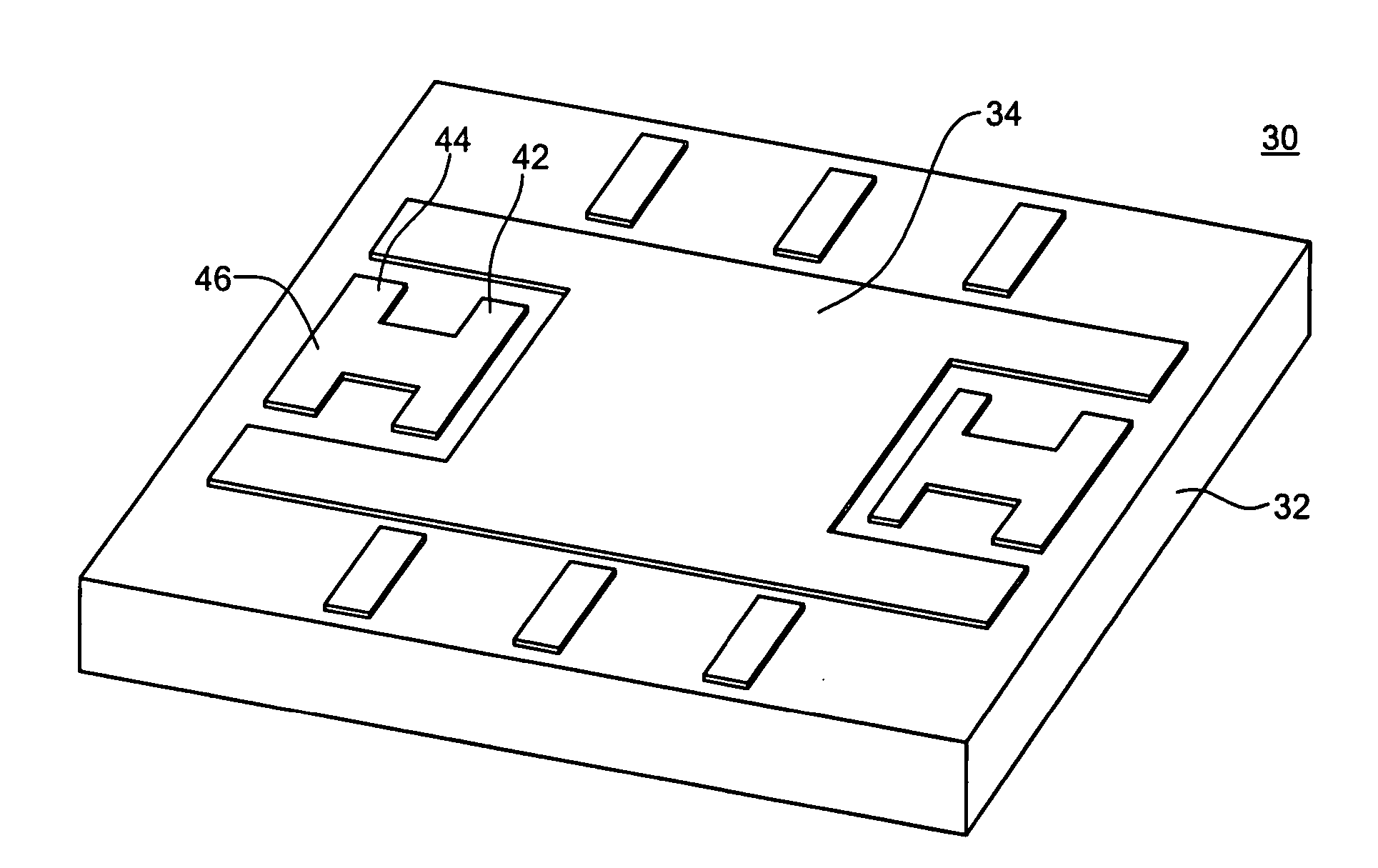
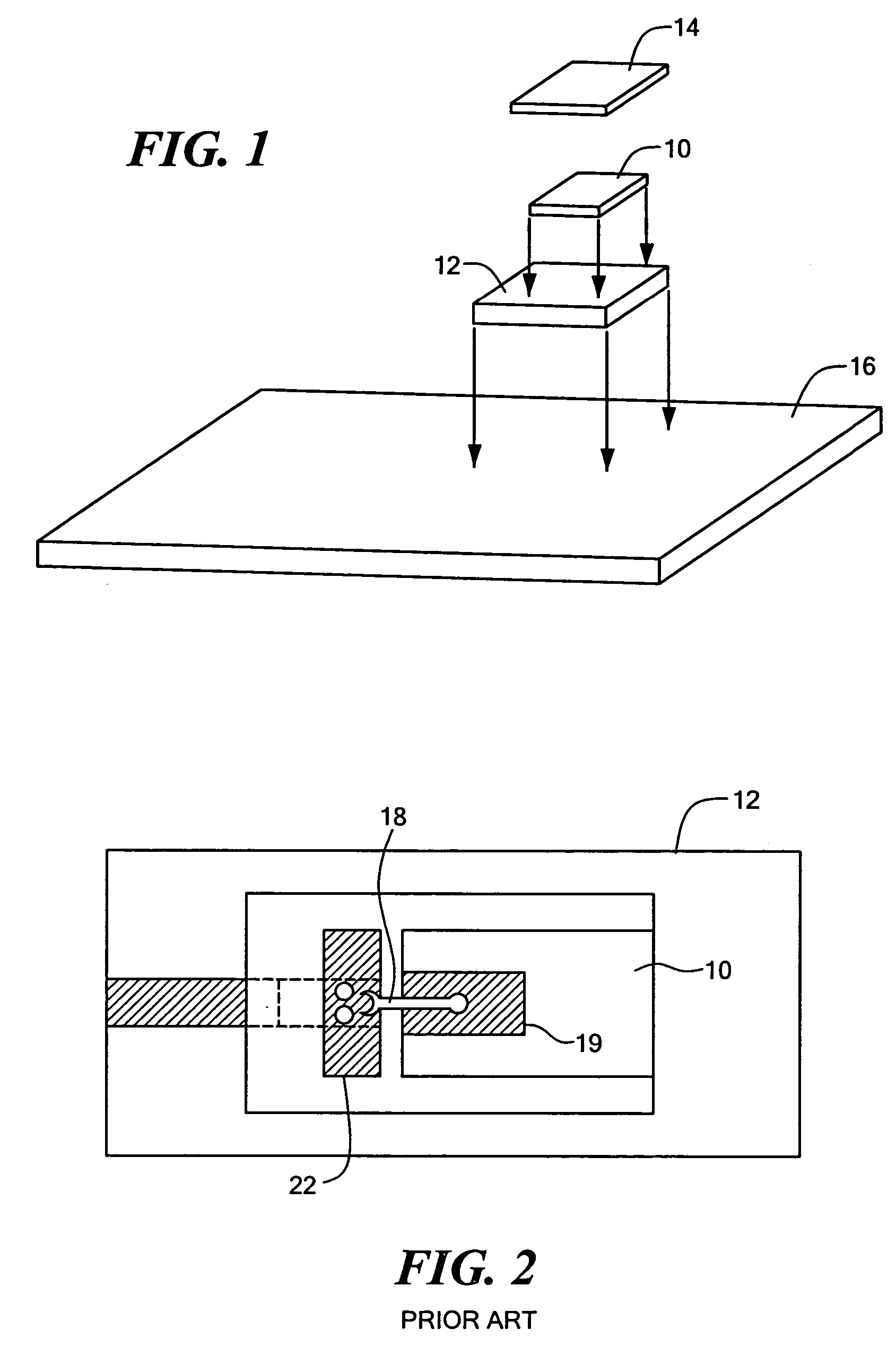
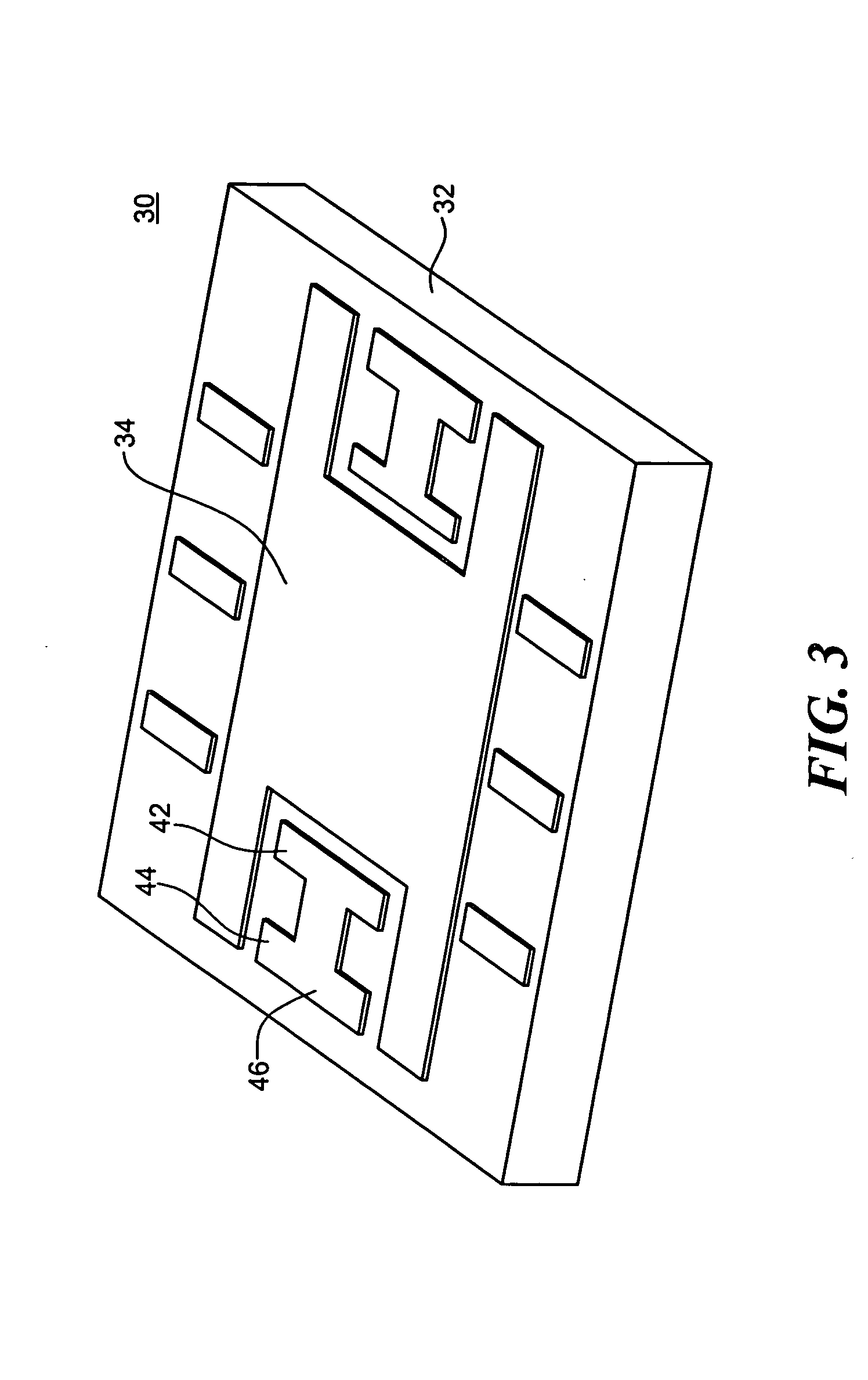
[0043] As disclosed in the background section above, an integrated circuit die such as a Monolithic Microwave Integrated Circuit (MMIC) 10, FIG. 1 is typically assembled into a package 12 including cover 14. The package is mounted on printed circuit board 16 using, for example, surface mount technology.

[0044] In the prior art, die 10, FIG. 2 is connected to package 12 using one or more wire bonds 18 which interconnect die port 19 of die 10 to bonding pad 22 on package 12 which is part of the transmission path. To reduce the effect of the parasitic inductance of wire bond 18, U.S. Pat. No...


PUM


Abstract

A novel package includes a substrate including an upper surface ground plane connected to a lower surface ground plane by vias through the substrate, a die located on the upper ground plane and including a die pad, a transmission path including, on the upper surface of the substrate, a bonding pad connected to a first transmission line itself connected to a transition pad, and on the lower surface of the substrate, a second transmission line connected to the transition pad by a via through the substrate. A wire bond extends from the bonding pad to the die pad. A portion of the upper surface ground plane and the lower surface ground plane are connected by vias defining opposing walls on either side of the transmission path for signal isolation. A low pass filter for compensating wire bond inductance includes: a first capacitance formed between the bonding pad and at least the lower surface ground plane, the wire bond inductance, and a second capacitance formed between the die pad and at least the upper surface ground plane.

Description

FIELD OF THE INVENTION [0001] This invention relates to a package useful in connection with monolithic microwave integrated circuits and exhibiting improved signal isolation and lower parasitic inductance. BACKGROUND OF THE INVENTION [0002] Integrated circuit dies such as a Monolithic Microwave Integrated Circuits (MMICs) are typically assembled into a package itself mounted on a printed circuit board (PCB) using, for example, surface mount technology. [0003] The die is electrically connected to the package using one or more wire bonds which interconnect a die pad on the die to a bonding pad on the package which is part of a transmission path. [0004] The wire bonds, however, have significant parasitic inductance which adversely affects the performance of the die especially at higher millimeter wave frequencies on the order of 20 GHz or more. [0005] Thus, those skilled in the art have previously attempted to reduce the effect of the parasitic inductance of the wire bonds. [0006] U.S....

Claims


Application Information

Patent Timeline
Patent Type & Authority Applications(United States)
IPC IPC(8): H01P1/04
CPCH01L23/66H01L2224/49111H01L2924/14H01L2924/1423H01L2924/19041H01L2924/30107H01L24/49H01P1/047H01L2924/3011H01L2224/48227H01L2924/00012H01L2924/30111H01L2924/00014H01L2224/45014H01L2924/00H01L2224/45015H01L2924/207H01L2924/206
Inventor ORAN, EKREM
Owner HITTITE MICROWAVE LLC
Why Eureka
Try Eureka