Systems for millimeter-wave chip packaging
a technology of millimeter-wave chips and packaging, applied in waveguides, semiconductor devices, semiconductor/solid-state device details, etc., can solve problems such as difficult channel isolation to prevent inter-channel loss or distortion, and achieve good multi-channel signal isolation
- Summary
- Abstract
- Description
- Claims
- Application Information
AI Technical Summary
Benefits of technology
Problems solved by technology
Method used
Image
Examples
embodiment 1
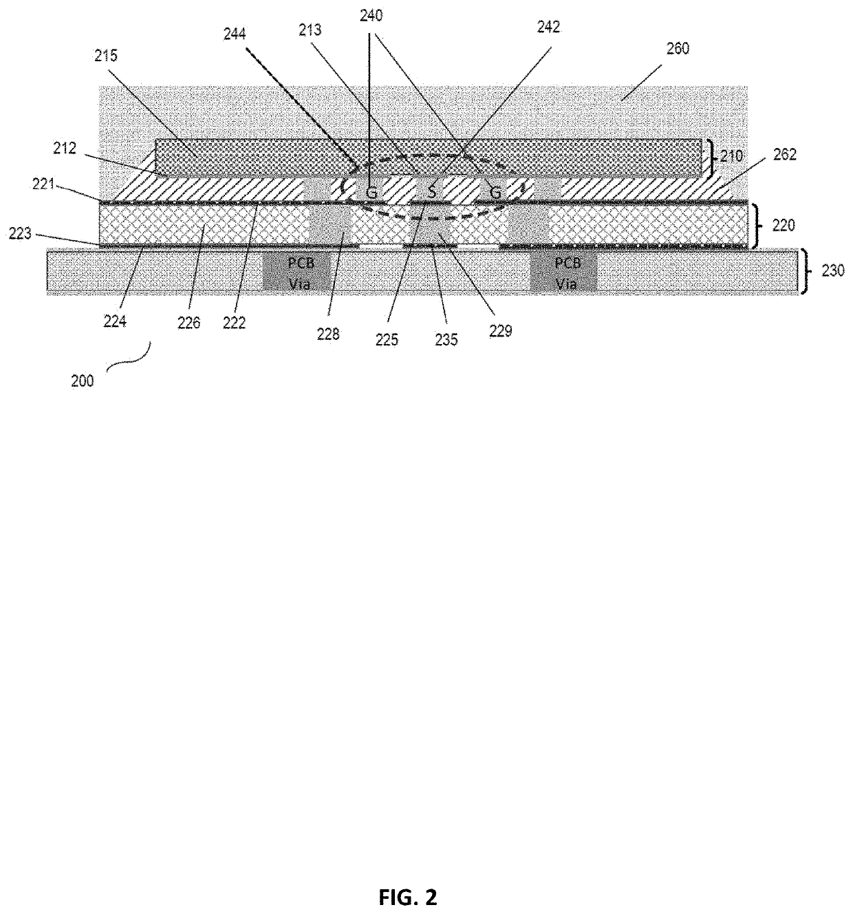
[0031]FIG. 2 depicts a cross-sectional view of a chip package 200 according to embodiment 1 of the invention. The chip package 200 comprises a chip 210 and a substrate 220. The substrate 220 comprises a top metal layer 221, a bottom metal layer 223, and an insulation layer 226 between the top metal layer and the bottom metal layer. The top metal layer comprises a top ground layer 222 and a first top signal strip 225. The bottom metal layer comprises a bottom ground layer 224 and a first bottom signal strip 235. The top ground layer and the bottom ground layer are electrically connected by one or more substrate vias 228 through the insulation layer 226. The first top signal strip 225 electrically insulated from the top ground layer 222. The chip 210 comprises a first ground plane 212 electrically connects to the top ground layer 222 via a plurality of metal pillars 240 deposited on the first ground plane 212. The chip 210 also comprises a first signal pad 213 electrically connected t...
embodiment 2
[0041]FIG. 8 depicts a cross-sectional view of a chip package with a second ground plane according to embodiment 2 of the invention. The chip 810 further comprises a first ground plane 811 and a second ground plane 812. The second ground plane 812 is positioned above the first signal path 820 and electrically connects the first ground plane via a plurality of on-chip metal-to-metal vias 814. With the second ground plane, the first CPW structure on the chip becomes a coplanar waveguide with ground (CPWG) structure 816, which provides enhanced interference immunity of the first signal path within the chip.
embodiment 3
[0042]FIG. 9 depicts a cross-sectional view of a chip package with multiple signal paths and a second ground plane according to embodiment 3 of the invention. The chip 910 further comprises a second signal path 904 separated from a first signal path 902 by a ground section 906. A second ground plane 912, electrically connected to a first ground plane (911a and 911b), and the ground section 906 via a plurality of on-chip metal-to-metal vias 914, is positioned above the first signal path 902 and the second signal path 904. Accordingly, a first CPWG structure 916 around the first signal path and a second CPWG structure 918 around the second signal path are formed. These two CPWG structures provide inter-path signal isolation within the chip through suppressing signal interference between signal paths due to leakage from chip substrate. A plurality of ground connected metal pillars 922 and 924 between the first and the second signal paths provide enhanced inter-path signal isolation thr...
PUM
| Property | Measurement | Unit |
|---|---|---|
| impedance | aaaaa | aaaaa |
| impedance | aaaaa | aaaaa |
| frequency | aaaaa | aaaaa |
Abstract
Description
Claims
Application Information


