Method of manufacturing a fin field effect transistor

Active Publication Date: 2005-08-25
SAMSUNG ELECTRONICS CO LTD
View PDF9 Cites 46 Cited by
  • Summary
  • Abstract
  • Description
  • Claims
  • Application Information

AI Technical Summary

Benefits of technology

[0012] Some embodiments of the invention provide a method of manufacturing a fin field effect transistor (fin FET), which is capable of increasing productivity by substantially reducing a manufacturing cost, without using an SOI type substrate that becomes a factor of high production cost.
[0013] Other embodiments of the inven

Problems solved by technology

A scaling-down of a general planar field effect transistor in conformity with the high-integration of the devices results in a lowered performance or reliability of the devices.
However, a fin FET manufacturing method according to a conventional technique has the following problems.
First, production costs of the SOI type silicon substrate is high, which results in increased manufacturing costs of the dev

Method used


Image

  • Method of manufacturing a fin field effect transistor
  • Method of manufacturing a fin field effect transistor
  • Method of manufacturing a fin field effect transistor

Examples


Embodiment Construction

[0017] Exemplary embodiments of the invention are more fully described in detail with reference to the accompanying drawings. The invention may be embodied in many different forms and should not be construed as being limited to the exemplary embodiments set forth herein. Rather, these exemplary embodiments are provided so that this disclosure is thorough and complete, and to convey the concept of the invention to those skilled in the art.

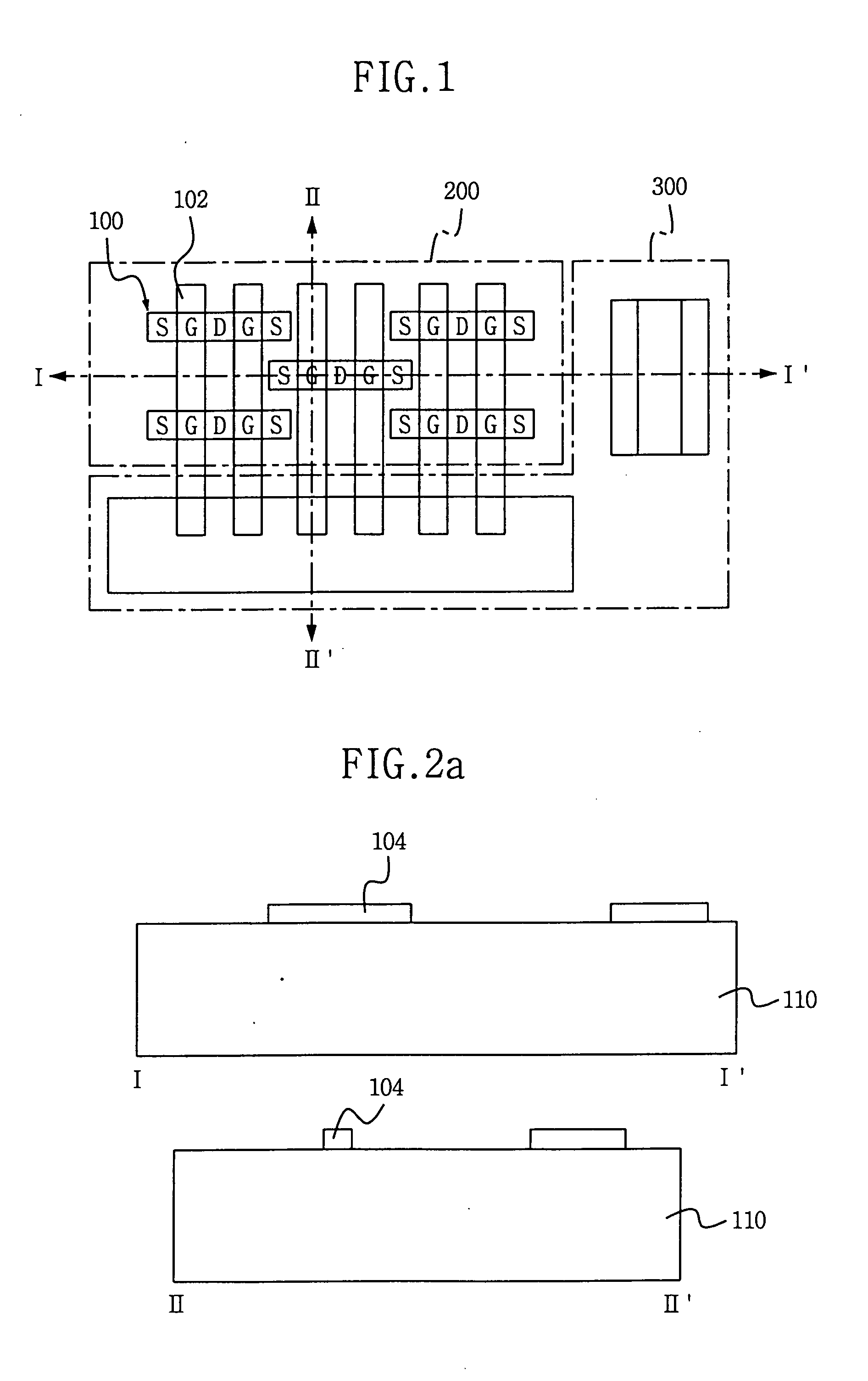
[0018]FIG. 1 is a plan view schematically illustrating a fin FET according to an exemplary embodiment of the invention.

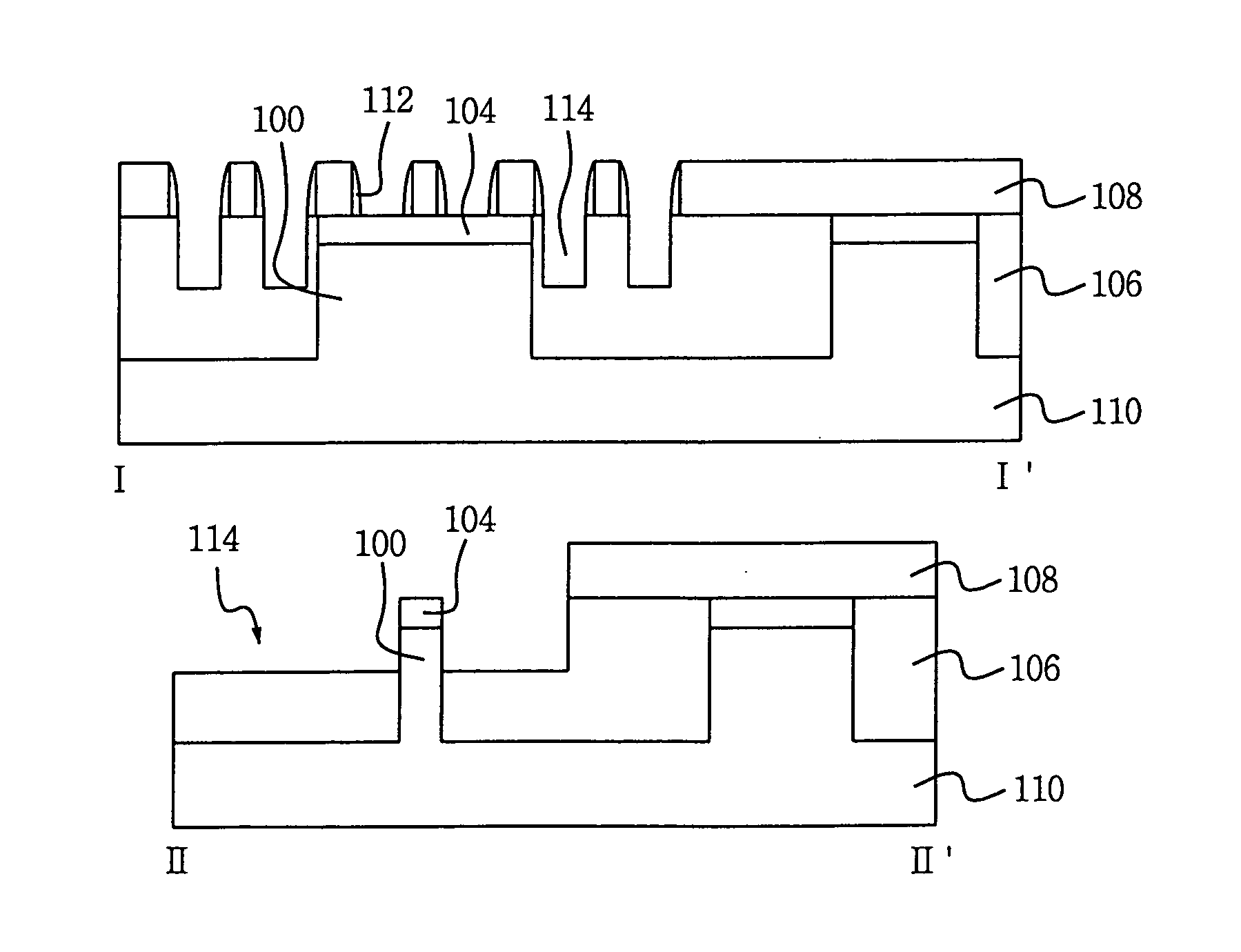
[0019] Referring to FIG. 1, a fin FET (Fin Field Effect Transistor) according to an exemplary embodiment of the invention is constructed of a fin active region 100 protruded from a bulk silicon substrate (110 of FIG. 2a) and arranged in one direction, and a gate line 102 crossing the fin active region 100. The fin active region 100 is constructed of a source region S and a drain region D provided on both sides thereof, centering o...


PUM


Abstract

In an exemplary embodiment, a fin active region is protruded along one direction from a bulk silicon substrate on which a shallow trench insulator is entirely formed so as to cover the fin active region. The shallow trench insulator is removed to selectively expose an upper part and sidewall of the fin active region, along a line shape that at least one time crosses with the fin active region, thus forming a trench. The fin active region is exposed by the trench and thereon a gate insulation layer is formed. Thereby, productivity is increased and performance of the device is improved. A fin FET employs a bulk silicon substrate of which a manufacturing cost is lower than that of a conventional SOI type silicon substrate. Also, a floating body effect can be prevented, or is substantially reduced.

Description

CROSS REFERENCE TO RELATED APPLICATIONS [0001] This application claims priority from Korean Patent Application No. 2004-11782, filed on Feb. 23, 2004, the contents of which are hereby incorporated by reference for all purposes. BACKGROUND OF THE INVENTION [0002] 1. Field of the Invention [0003] This disclosure relates to semiconductor devices, and more particularly, to a method of manufacturing a fin field effect transistor. [0004] 2. Description of the Related Art [0005] Recent rapid development in the information and communication field, and a popularization of information media such as computers, have brought about a rapid progress of semiconductor devices. A high-integration of semiconductor devices has brought about research activity for various methods of reducing a feature size of individual devices formed on a substrate while increasing performance of the devices. [0006] In such methods a field effect transistor (FET) is increasingly used to improve integration of devices ba...

Claims


Application Information

Patent Timeline
IPC IPC(8): H01L29/78H01L21/336H01L21/8242H01L27/108H01L29/786
CPCH01L27/10823H01L27/10826H01L29/7851H01L27/10879H01L29/66795H01L27/10876H10B12/36H10B12/34H10B12/056H10B12/053H01L29/66719H01L29/4232H01L29/42312H01L29/66583
Inventor LEE, CHULYOON, JAE-MANLEE, CHOONG-HO
Owner SAMSUNG ELECTRONICS CO LTD
Why Eureka
Try Eureka