Semiconductor integrated circuit having a power-on reset circuit in a semiconductor memory device

a technology of integrated circuit and reset circuit, which is applied in the direction of digital storage, instruments, and increasing modifications to ensure reliability, and can solve problems such as the inability to properly reset other internal circuits

Inactive Publication Date: 2005-09-01
OKI ELECTRIC IND CO LTD
View PDF4 Cites 16 Cited by
  • Summary
  • Abstract
  • Description
  • Claims
  • Application Information

AI Technical Summary

Benefits of technology

[0010] An object of the present invention is to properly reset the internal circuit which operates based on the output signal from the internal circuit which needs not to be reset when the power supply voltage is generated.

Problems solved by technology

Therefore, on such an occasion as this, the other internal circuit may not be properly reset.

Method used


Image

  • Semiconductor integrated circuit having a power-on reset circuit in a semiconductor memory device
  • Semiconductor integrated circuit having a power-on reset circuit in a semiconductor memory device
  • Semiconductor integrated circuit having a power-on reset circuit in a semiconductor memory device

Examples


Embodiment Construction

[0040] Embodiments of the present invention will be described hereinafter with references to the accompanying drawings. The drawings used for this description illustrate major characteristic parts of embodiments in order that the present invention will be easily understood. However, the invention is not limited by these drawings.

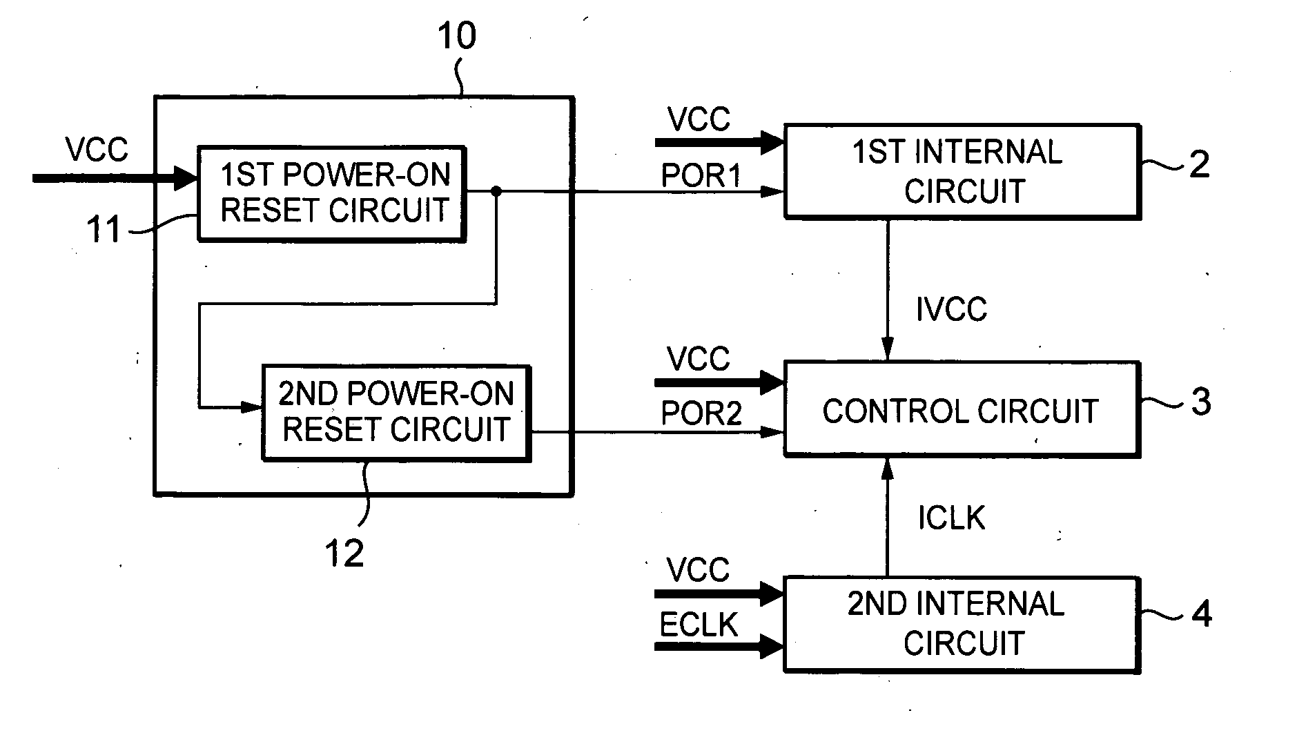
[0041]FIG. 4 is a schematic circuit diagram for describing a semiconductor integrated circuit of a semiconductor memory device according to a first preferred embodiment of the present invention. This semiconductor integrated circuit has a first internal circuit 2, a control circuit 3, a second internal circuit 4 and a power-on reset circuit 10 which all receives a power supply voltage Vcc. For example, an internal power supply voltage generating circuit is used as the first internal circuit 2, and an internal clock generating circuit is used as the second internal circuit 4.

[0042] The first internal circuit 2 generates an internal power supply voltage IVcc...


PUM


Abstract

A semiconductor integrated circuit, which operates in accordance with a power supply voltage and an external clock signal and includes a memory circuit, includes a control circuit, and first and second internal circuits. The control circuit controls the memory circuit in accordance with the power supply voltage. The first internal circuit generates an internal power supply voltage for the control circuit. The second internal circuit generates an internal clock signal for the control circuit. The semiconductor integrated circuit further includes first and second power-on reset circuits. The first power-on reset circuit generates a first power-on reset signal for the first internal circuit after the power supply voltage is generated. The second power-on reset circuit generates a second power-on reset signal for the control circuit. The second power-on reset signal is input to the control circuit after the internal clock signal is input to the control circuit.

Description

BACKGROUND OF THE INVENTION [0001] 1. Field of the Invention [0002] The present invention relates to a semiconductor integrated circuit, and in particular, to a semiconductor integrated circuit including a power-on reset circuit which resets an internal circuit in a semiconductor memory device during a start-up process of the semiconductor integrated circuit. This is a counterpart of and claims priority to Japanese Patent Application No. 2004-51894 filed on Feb. 26, 2004, which is herein incorporated by reference. [0003] 2. Description of the Related Art [0004]FIG. 1 is a block diagram for describing a semiconductor integrated circuit in a semiconductor memory device of the related art. The semiconductor integrated circuit comprises a power-on reset circuit 100, an internal voltage generating circuit 200, a control circuit 300 and an internal clock generating circuit 400. A power supply voltage Vcc is externally input to the power-on reset circuit 100, the internal voltage generatin...

Claims


Application Information

Patent Timeline
Patent Type & Authority Applications(United States)
IPC IPC(8): H03K19/003G11C11/401H03K3/037H03K3/354H03K17/22H03K19/0175H03L7/00H03L7/08
CPCH03L7/08H03K17/223
Inventor NAKATAKE, YOSHIHIRONARUMI, AKIHIRO
Owner OKI ELECTRIC IND CO LTD
Why Eureka
Try Eureka