

Method and apparatus for rapid prototyping of monolithic microwave integrated circuits
a monolithic microwave integrated circuit and prototyping method technology, applied in amplifiers, amplifiers with semiconductor devices/discharge tubes, amplifiers, etc., can solve the problem that satisfaction for prototyping purposes is not necessarily desirable, and achieve the effect of reducing costs
- Summary
- Abstract
- Description
- Claims
- Application Information
AI Technical Summary
Benefits of technology
Problems solved by technology
Method used
Image

Examples
Embodiment Construction
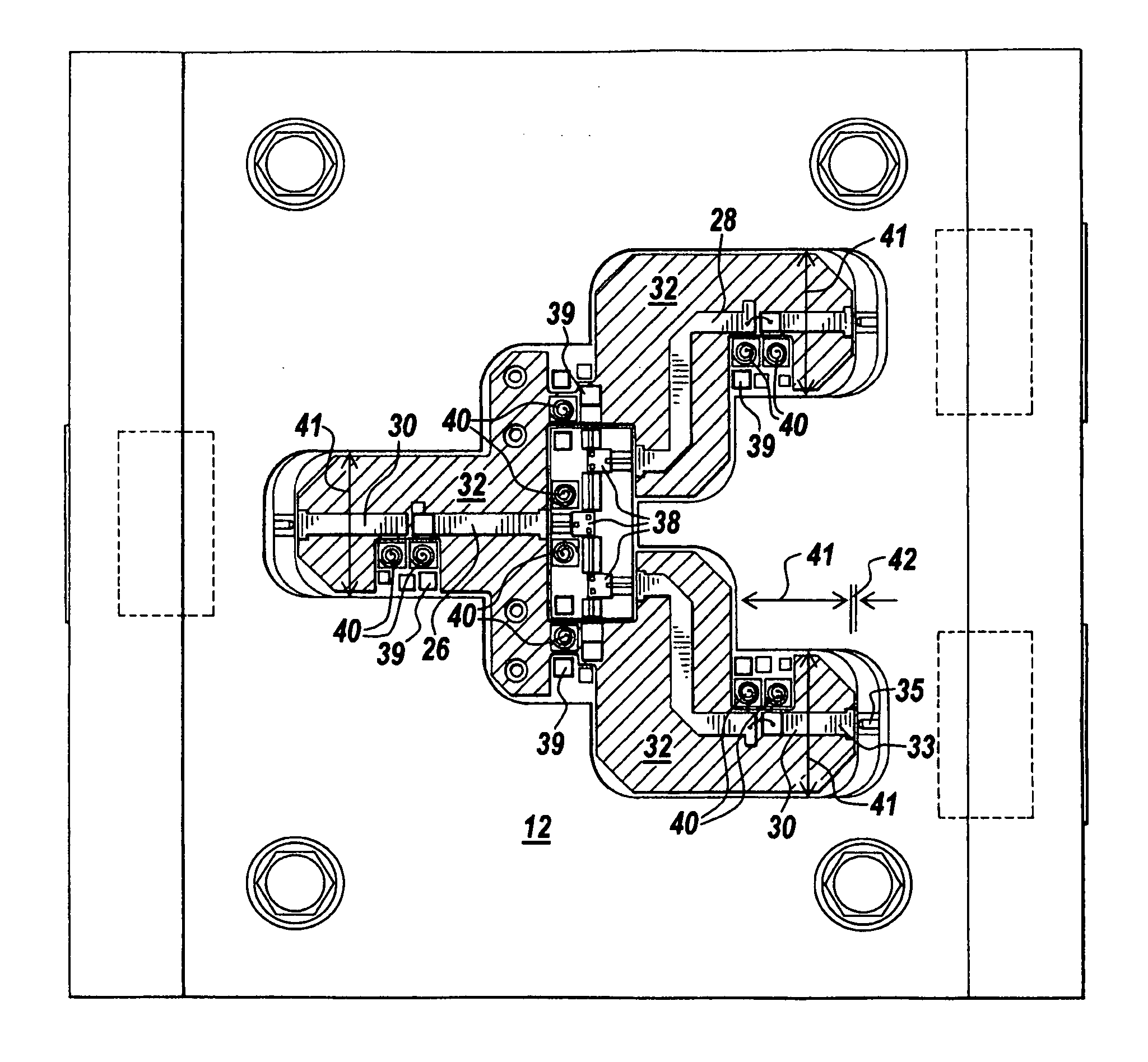
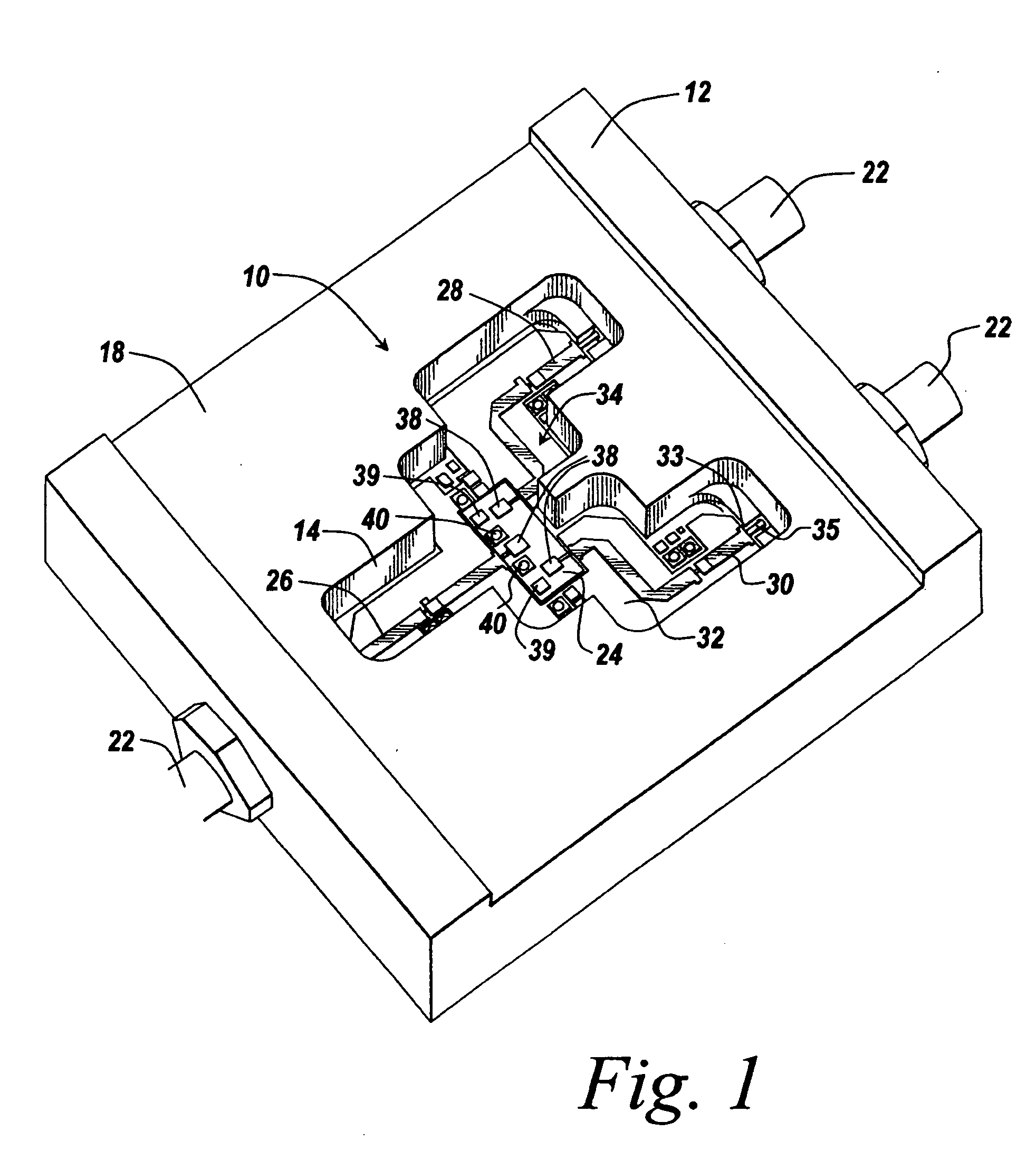
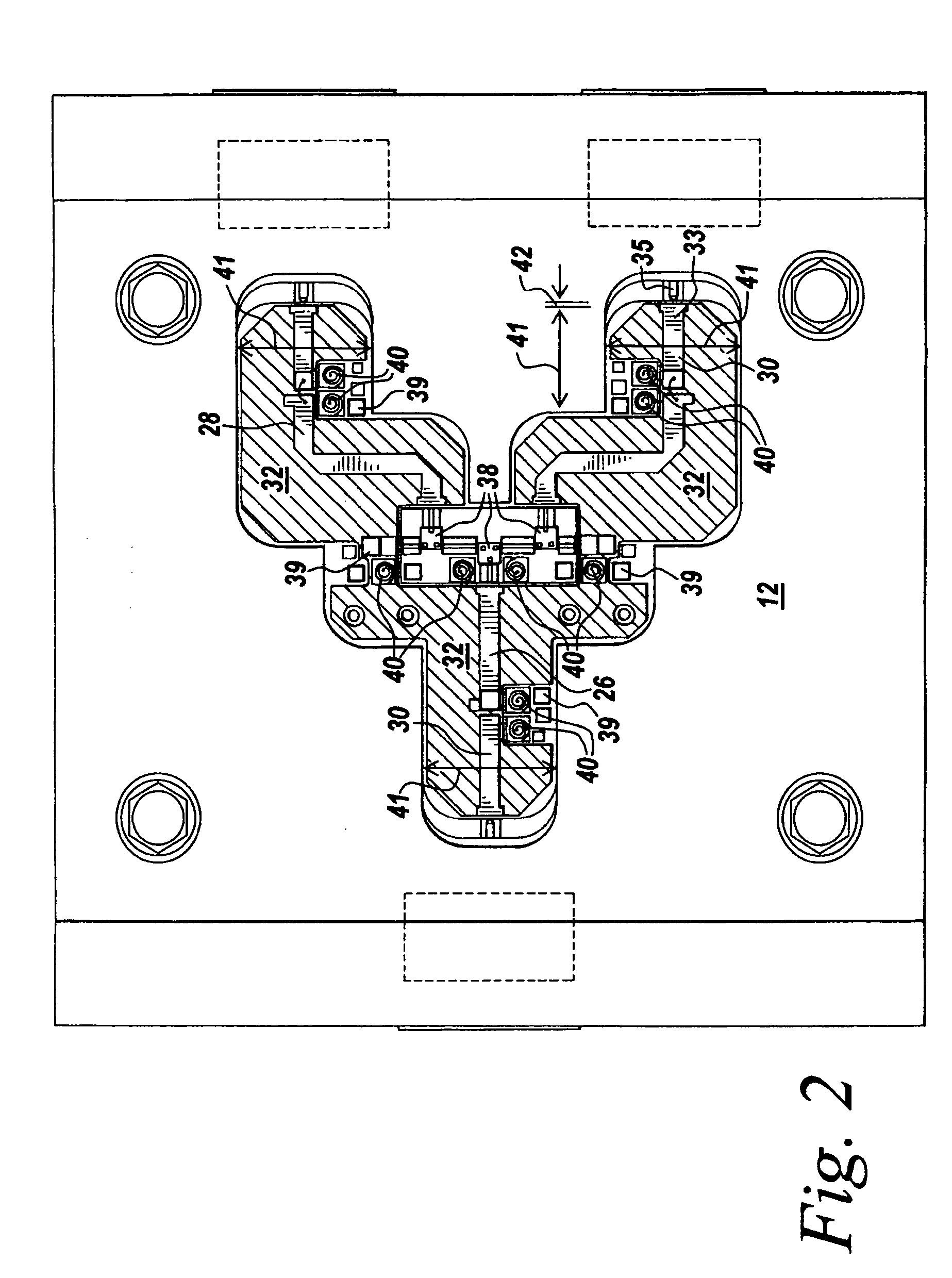
[0024] Prior to discussing the housing and the criticality of the dimensions, it will be appreciated that microwave integrated circuits have components such as conductors, inductors, capacitors, resistors and active circuits which must be positioned relative to the housing with tolerances in the range of thousandths of an inch. What this means is that when one seeks to design a housing into which the components are to fit, there are some critical dimensions which become operative due to the microwave frequencies.
[0025] Rather than simply locating components on a circuit board in an indiscriminate fashion, one needs to pay attention to various dimensions because the wavelengths are so short. If the placement of a part or positioning of a line or trace is inconsistent with good design practice, the performance of the circuit can be degraded or can even be unacceptable.
[0026] For instance, misplacement of the components may cause detuning and may cause undesirable reflections, becaus...
PUM
| Property | Measurement | Unit |
|---|---|---|
| Ra | aaaaa | aaaaa |
| thickness | aaaaa | aaaaa |
| smoothness | aaaaa | aaaaa |
Abstract
Description
Claims
Application Information