Subfield coding circuit, image signal processing circuit, and plasma display

a signal processing circuit and subfield coding technology, applied in the field of subfield coding circuits, image signal processing circuits, and plasma displays, can solve the problems of reducing image quality, moving image false contouring, and the maximum possible memory capacity is not as high as that of the dedicated dram chip, sram b>161/b> used, etc., to achieve high speed operation, reduce memory capacity, and reduce the area of the lsi chip

Inactive Publication Date: 2005-09-01
PIONEER CORP
View PDF8 Cites 19 Cited by
  • Summary
  • Abstract
  • Description
  • Claims
  • Application Information

AI Technical Summary

Benefits of technology

[0065] It is an object of the present invention to provide a subfield coding circuit, an image signal processing circuit, and a plasma display which allow a reduction in memory capacity.
[0066] It is another object of the present invention to provide a subfield coding circuit, an image signal processing circuit, and a plasma display which are capable of high speed operation.
[0067] It is still another object of the present invention to provide a subfield coding circuit, an image signal processing circuit, and a plasma display which allow a reduction in the area of the LSI chip.

Problems solved by technology

There has been the problem that when the gradation rendering is achieved by using the SFs divided as many as the number of bits of the input image signal (image data) as described above, there may occur a degradation in image quality called a moving-image false contouring.
The DRAM has the disadvantage, however, that the maximum possible memory capacity is not as high as that of the dedicated DRAM chip (external memory).
The image signal processing circuit according to the second prior art example, however, has the problem that the SRAMs 161 used as the LUT memory of the SF coding circuit 232 increase in memory capacity.

Method used


Image

  • Subfield coding circuit, image signal processing circuit, and plasma display
  • Subfield coding circuit, image signal processing circuit, and plasma display
  • Subfield coding circuit, image signal processing circuit, and plasma display

Examples


Embodiment Construction

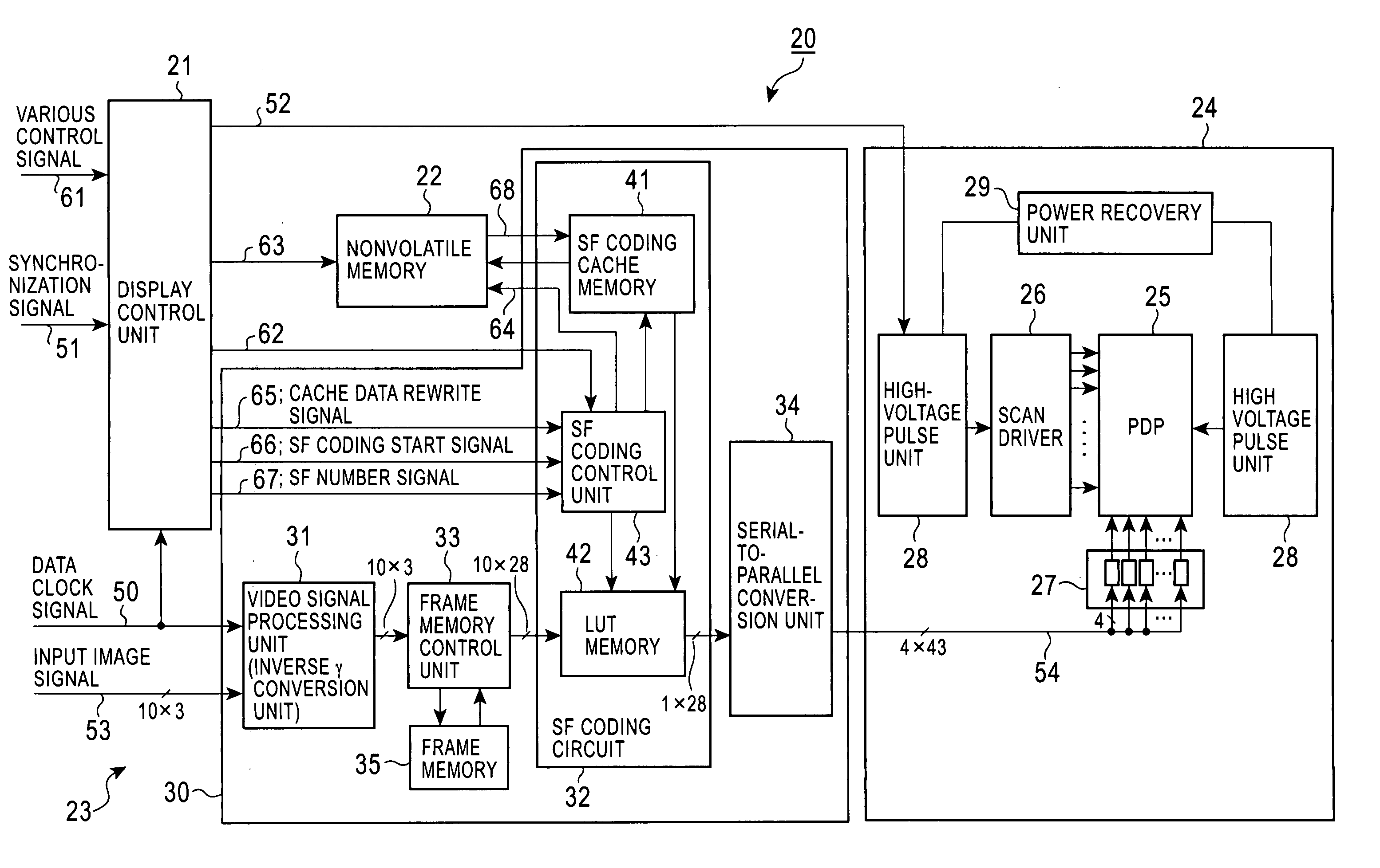
[0096] Hereinafter, the best mode for carrying out the plasma display according to the present invention will be described with reference to the accompanying drawings.

[0097]FIG. 5 is a block diagram showing the configuration of a plasma display 20 according to the present invention. The plasma display 20 of the present invention includes a display control unit 21, an image signal processing circuit 30, and a display device (display unit) 24. The image signal processing circuit 30 is implemented on a signal processing LSI 23 (signal processing LSI chip 23).

[0098] A data clock signal 50 is input to the display control unit 21 and the image signal processing circuit 30.

[0099] A synchronization signal 51 is input to the display control unit 21. The display control unit 21 outputs a scan driver control signal 52 to the display device 24 in accordance with the data clock signal 50 and the synchronization signal 51.

[0100] Input image signals 53 are input to the image signal processing ...


PUM


Abstract

A subfield (SF) coding circuit including an SF coding cache memory, a look-up table (LUT) memory, and an SF coding control unit. The coding control unit reads setting gradation values and SF coding data from the coding cache memory for writing to the LUT memory SF by SF. The control unit accesses the LUT memory by using the gradation value of an image signal from a frame memory control unit as an address, and outputs the SF coding data corresponding to the gradation value of the image signal input to the LUT memory to a serial-to-parallel conversion unit.

Description

BACKGROUND OF THE INVENTION [0001] 1. Field of the Invention [0002] The present invention relates to a subfield coding circuit for converting an input image signal (RGB image signal) into subfield coding data, an image signal processing circuit, and a plasma display apparatus. [0003] 2. Description of the Related Art [0004] Among examples of display devices having a flat-panel display are plasma display panels (PDPs), organic / inorganic electroluminescence (EL) panels, and projection panels using direct mirror devices (DMDs). [0005] In these display devices, each individual display cell can only take two values, or “light emission” and “non-emission.” Tone gradations are thus rendered by controlling the numbers of times of light emission from the respective display cells. Take, for example, the case of 8-bit tone or 8-bit gradation rendering with R (red), G (green), and B (blue) display cells for use in color display. The numbers of times of light emission from the respective display...

Claims


Application Information

Patent Timeline
Patent Type & Authority Applications(United States)
IPC IPC(8): H04N5/66G09G3/20G09G3/28G09G3/296
CPCG09G3/2022G09G2360/121G09G3/28G09G3/288A47K11/035E04H1/1216
Inventor MANABE, TAKASHI
Owner PIONEER CORP
Why Eureka
Try Eureka