Drive device and drive method of light emitting display panel

a technology of drive device and display panel, which is applied in the direction of static indicating device, electroluminescent light source, instruments, etc., can solve the problems of increasing the occupying volume of capacitors, increasing the cost, and increasing the occupying volume of capacitors, so as to increase the circuit scale and improve the display quality of images. , the effect of increasing the occupying volum

Active Publication Date: 2005-09-01
TOHOKU PIONEER CORP
View PDF1 Cites 12 Cited by
  • Summary
  • Abstract
  • Description
  • Claims
  • Application Information

AI Technical Summary

Benefits of technology

[0028] The present invention has been developed as attention to the above-described problems has been paid, and it is an object of the present invention to provide a drive device and a drive method of a light emitting display panel in which deterioration of the display quality of an image caused by a ripple component generated in a power supply circuit represented by a DC-DC converter can be effectively reduced without increasing the circuit scale so much.

Problems solved by technology

Particularly, although the demand for the display panel and the DC-DC converter driving this display panel which are shown in FIG. 1 is increasing due to the spread of cellular phones, personal digital assistants (PDAs), and the like, employing a large capacitance smoothing capacitor for this type of equipment not only increases the cost but also increases the occupying volume of the capacitor.
Thus, in the display panel, a problem that the display quality of an image is considerably deteriorated, that is, for example, a fine striped pattern or phenomenon of flicker occurs and the like, can occur.
However, in the regulator circuit, a power loss of (Vin−Vout)×Iout=P[W] always occurs.
Accordingly, due to a problem that the continuous utilization time of a battery is drastically shortened, it is difficult to adopt such a device in the above-mentioned portable equipment under actual conditions.

Method used


Image

  • Drive device and drive method of light emitting display panel
  • Drive device and drive method of light emitting display panel
  • Drive device and drive method of light emitting display panel

Examples


Embodiment Construction

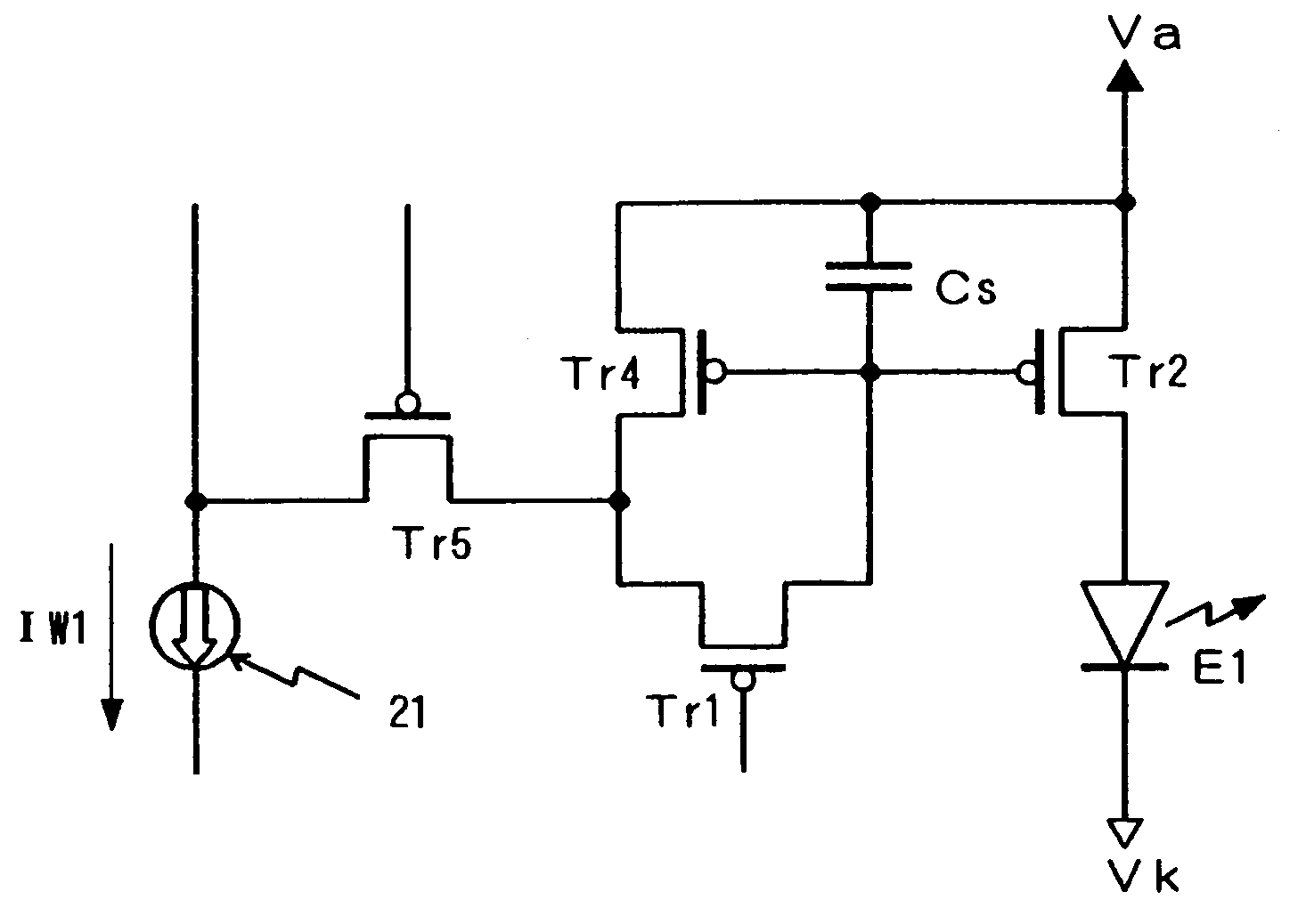
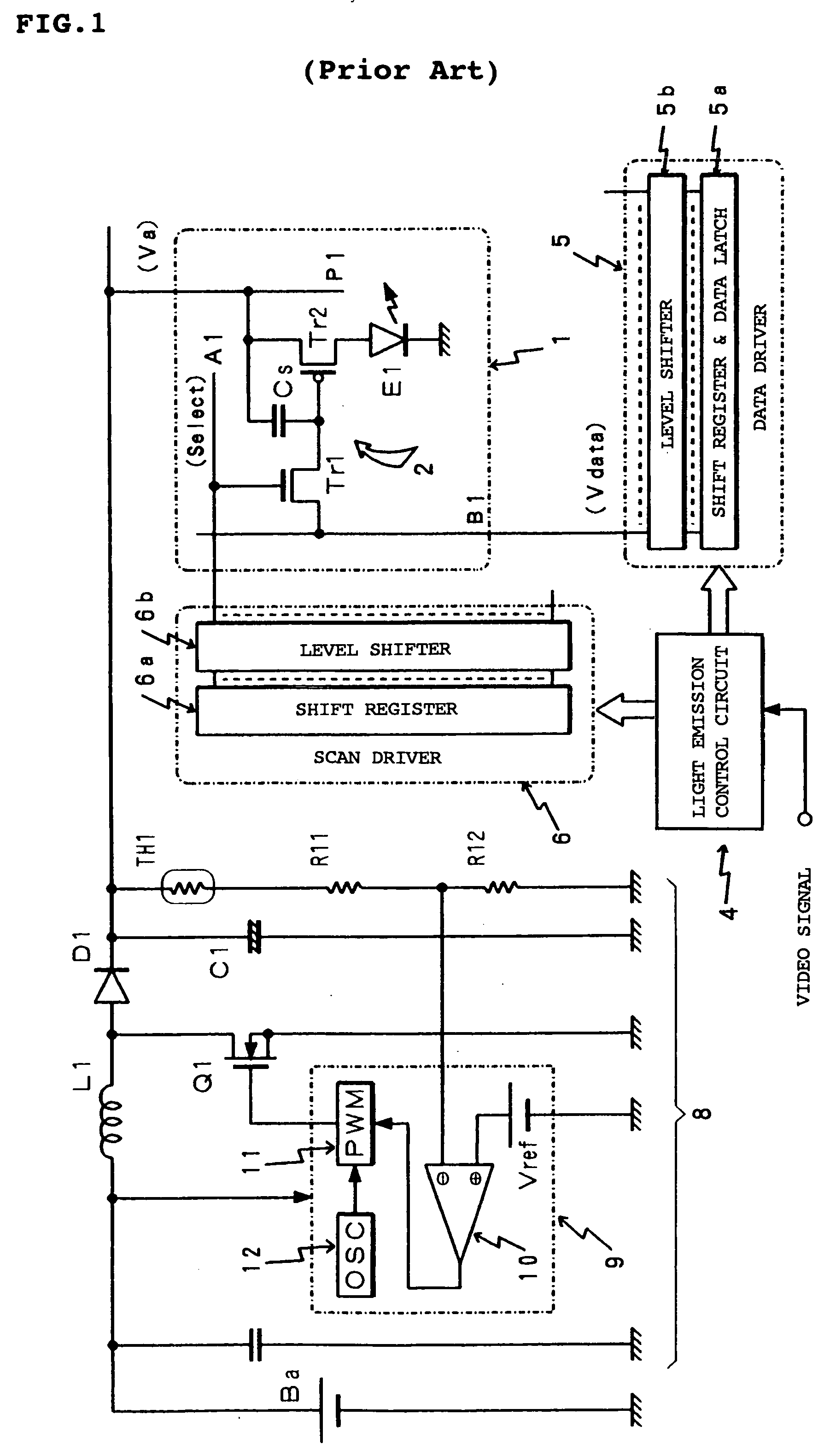
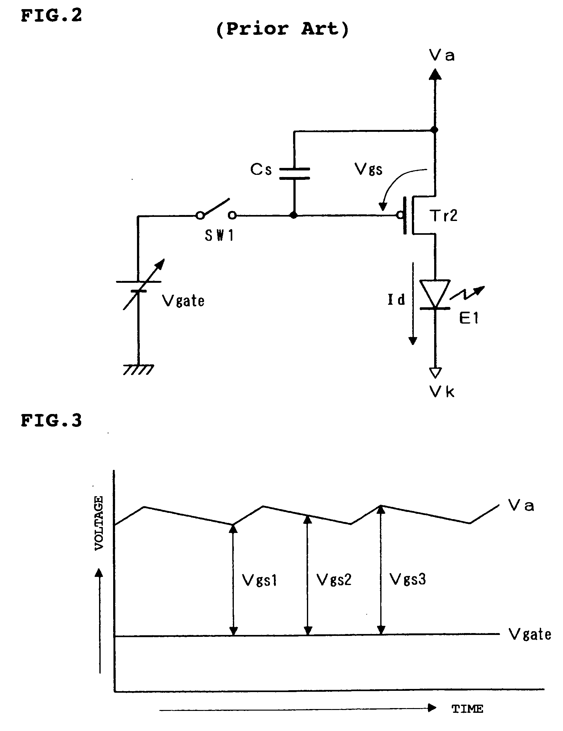
[0047] A drive device of a light emitting display panel according to the present invention will be described below with reference to the embodiments shown in the drawings. FIG. 6 shows a first embodiment of a drive device according to the present invention and shows a structure which is allowed to have ripple component supply means that the present invention is characterized, in a pixel structure of a conductance control method, similarly to the equivalent circuit shown in FIG. 2 already described. In the equivalent circuit of a pixel shown in FIG. 6, parts which perform the same functions as those of the respective parts shown in FIG. 2 are designated by the same reference characters, and detailed description thereof will be omitted.

[0048] In the embodiment shown in FIG. 6, a ripple component extraction circuit 14 and a voltage addition circuit 15 are provided and are constituting the ripple component supply means. The ripple component extraction circuit 14 extracts a ripple compo...


PUM


Abstract

The ripple component superimposed on the drive power source Va applied to the source electrode of a light emission drive transistor Tr2 is extracted by a ripple component extraction circuit 14, and the ripple component is supplied to one input terminal of a voltage addition circuit 15. A data voltage Vdata transmitted via a data line is input to the other input terminal of the voltage addition circuit 15. Accordingly, in the voltage addition circuit 15, the ripple component extracted by the ripple component extraction circuit 14 is added to the data voltage Vdata treating the data voltage Vdata as the base. Its output is supplied to a scan selection transistor designated by reference character SW1 as Vgate, and the transistor Tr1 is turned on at an addressing time so that the Vgate is supplied to the gate of the light emission drive transistor Tr2. Thus, the gate-to-source voltage Vgs of the light emission drive transistor Tr2 represents an approximately constant value all the time regardless of timing of addressing. Therefore, a problem that intensity change occurs for each scan line so that the display quality of an image is considerably deteriorated can be avoided.

Description

BACKGROUND OF THE INVENTION [0001] 1. Field of the Invention [0002] The present invention relates to a drive device of a display panel in which light emitting elements constituting pixels are actively driven for example by TFTs (thin film transistors), and more particularly to a drive device and a drive method of a display panel in which display quality of an image which is caused by a ripple component superimposed onto the drive power source of the light emitting elements can be prevented from deteriorating. [0003] 2. Description of the Related Art [0004] A display employing a display panel constructed by arranging light emitting elements in a matrix pattern has been developed widely, and as the light emitting element employed in such a display panel, for example, an organic EL (electroluminescent) element in which an organic material is employed in a light emitting layer has attracted attention. This is because of backgrounds one of which is that by employing, in the light emittin...

Claims


Application Information

Patent Timeline
Patent Type & Authority Applications(United States)
IPC IPC(8): G09G3/20H01L51/50G09G3/30H05B33/14
CPCG09G3/3266G09G2310/0289G09G2330/028G09G2320/0247G09G2320/0209
Inventor HAYAFUJI, AKINORI
Owner TOHOKU PIONEER CORP
Why Eureka
Try Eureka