Built-in self test method and apparatus for jitter transfer, jitter tolerance, and FIFO data buffer

a self-testing, fifo data technology, applied in the field of electronic equipment, can solve the problems that cannot be tested during manufacturing test today, and achieve the effect of easy testing of tx fifo

Inactive Publication Date: 2005-09-01
TEXAS INSTR INC
View PDF6 Cites 62 Cited by
  • Summary
  • Abstract
  • Description
  • Claims
  • Application Information

AI Technical Summary

Benefits of technology

[0013] Coincidentally, the BIST mechanism built to test the jitter tolerance and transfer also makes it possible to easily test the TX FIFO.

Problems solved by technology

Jitter tolerance and jitter transfer are important specifications to be met for transceivers but due to limitations of the automatic test equipment (ATE) available, these can not be tested for during manufacturing test today.

Method used


Image

  • Built-in self test method and apparatus for jitter transfer, jitter tolerance, and FIFO data buffer
  • Built-in self test method and apparatus for jitter transfer, jitter tolerance, and FIFO data buffer
  • Built-in self test method and apparatus for jitter transfer, jitter tolerance, and FIFO data buffer

Examples


Embodiment Construction

[0024] The making and using of the presently preferred embodiments are discussed in detail below. It should be appreciated, however, that the present invention provides many applicable inventive concepts that can be embodied in a wide variety of specific contexts. The specific embodiments discussed are merely illustrative of specific ways to make and use the invention, and do not limit the scope of the invention.

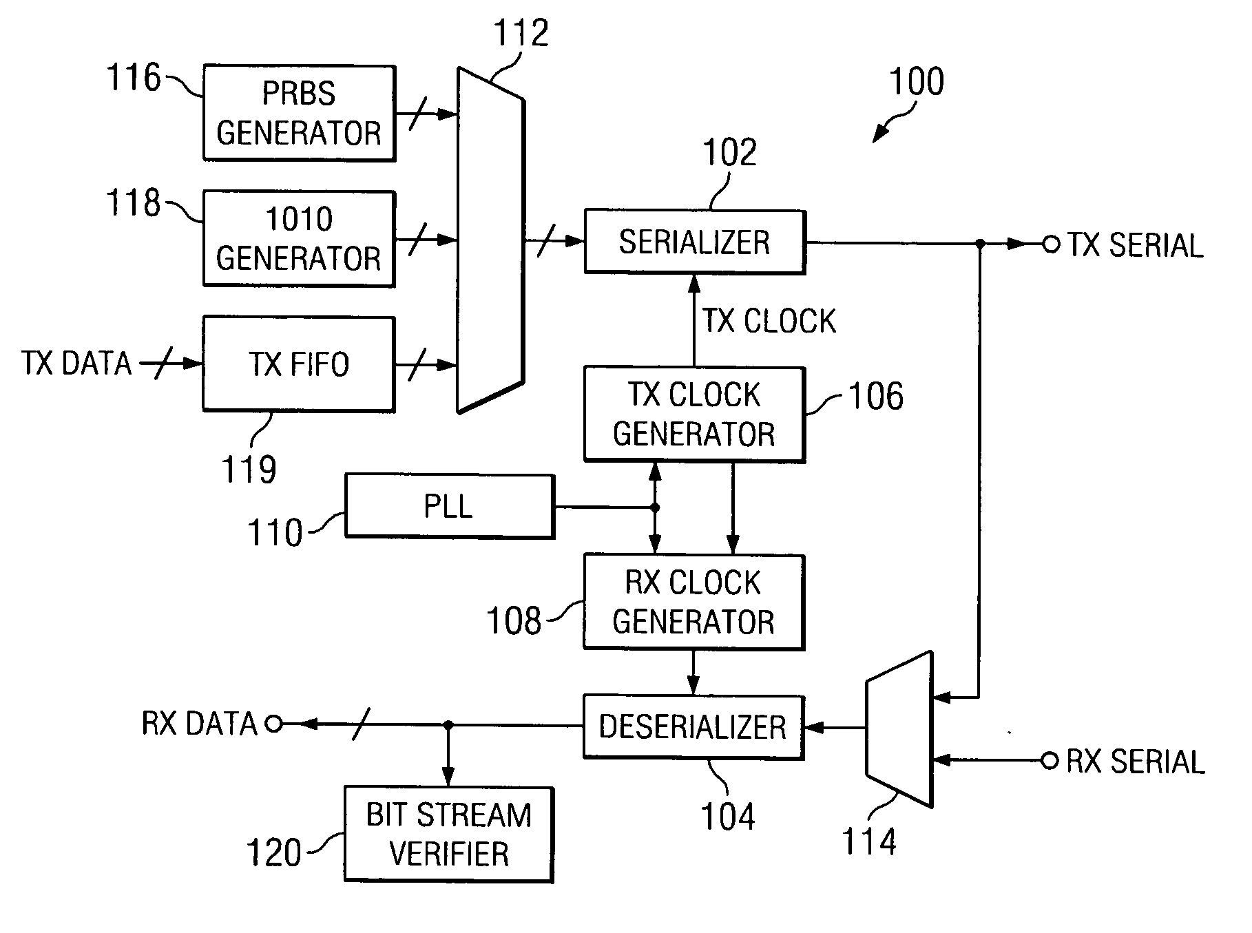
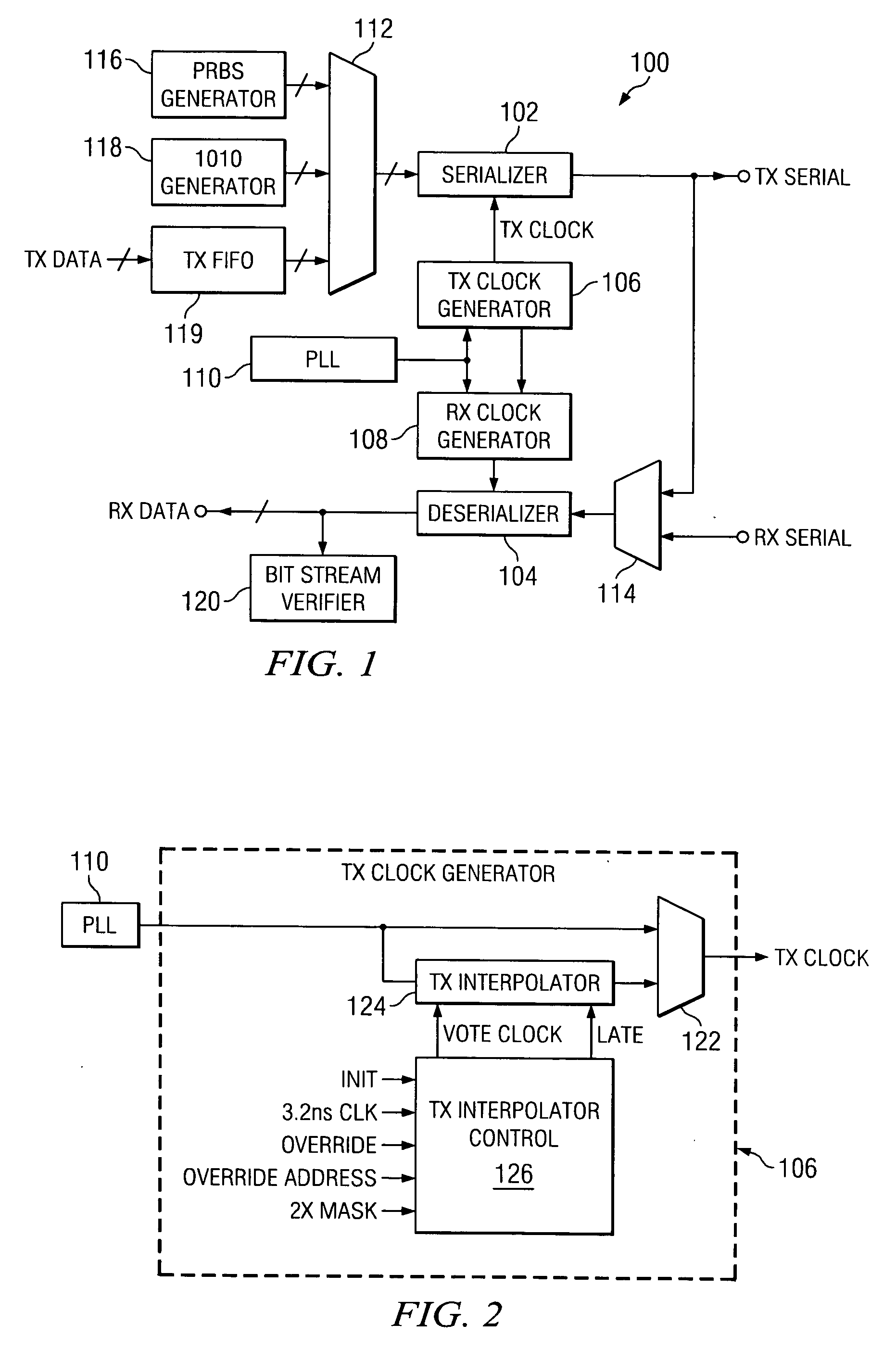
[0025] In one aspect, the present invention provides a method and apparatus to test for jitter tolerance and jitter transfer on a transceiver chip itself. For example, a transmitter side interpolator can be used to generate a desired jitter pattern. Serial data from the transmitter side can be looped back to the receiver's serial input. A pseudo-random binary sequence (PRBS) generation / verification mechanism can then be used to check jitter tolerance. Jitter transfer can be measured using an up / down counter to monitor receiver interpolator activity.

[0026] To test for jitte...


PUM


Abstract

Testing a transceiver includes providing a sequence of test signals. A serialization clock is generated and jitter is added to the clock in a known and controlled manner. The test signals can then be transmitted using the serialization clock. After the test signals are recovered by the clock and data recovery mechanism, the recovered sequence is compared to the original sequence, to test for jitter tolerance. Preferably, each of these steps is performed on chip. In other aspects, a jitter transfer test and/or a FIFO test can be performed.

Description

TECHNICAL FIELD [0001] The present invention relates to the field of electronic circuits, and more specifically, to a built-in self test method and apparatus for electronic equipment. BACKGROUND [0002] Many electronic components, such as transceivers, receive and / or transmit data at high speed. In particular, a transceiver, such as a serializer / deserializer (SERDES), can receive data in parallel form at an input and provide serial data at an output and vice versa. For example, a system might include two components that process data in parallel and are coupled to one another by a serial link. To transfer information from one component to the other, the first system would convert the parallel data to serial data and place the data on a transmission medium. Upon receipt at the second component, the data would be reconverted from the serial form to parallel form for processing at the second component. [0003] One of the design goals of the transceivers is to ensure that the data received...

Claims


Application Information

Patent Timeline
Patent Type & Authority Applications(United States)
IPC IPC(8): G01R31/317G11C29/00H03B19/00H04B17/00
CPCG01R31/31709G01R31/31715H04B17/20H04B17/0085H04B17/10G01R31/31725
Inventor CHO, JAMES B.BHAKTA, BHAVESH G.
Owner TEXAS INSTR INC
Why Eureka
Try Eureka