Charge pump circuit using active feedback controlled current sources

a current source and pump circuit technology, applied in the direction of pulse automatic control, power conversion system, dc-dc conversion, etc., can solve the problem of significant reduction of the preference spur exhibited by prior art designs, achieve high overdrive gate voltage, reduce noise contribution to the pll loop, and fast switching speed

Active Publication Date: 2005-09-08
REALTEK SEMICON CORP +1
View PDF9 Cites 40 Cited by
  • Summary
  • Abstract
  • Description
  • Claims
  • Application Information

AI Technical Summary

Benefits of technology

[0010] In accordance with preferred embodiments of the invention, the current sources of a charge pump circuit are regulated by active feedback control to match the currents that are driven into and out of the charge pump output node. Active feedback control may be implemented using voltage regulation devices that control the drain voltages of current source transistors so that the currents produced by the current source transistors mirror a reference current. This significantly reduces the preference spur exhibited by prior art designs.
[0011] Charge pump circuits in accordance with preferred embodiments of the invention also utilize multiple supply voltages. The current source transistors may be operated in the linear range, and a higher supply voltage such as a 3.3 V supply voltage may be used to drive the current source transistors, thus providing a high overdrive gate voltage that reduces the noise contribution to the PLL loop. A lower supply voltage such as a 1.8 V supply voltage may be used to drive the switches, which enables the switches to be implemented using very small critical dimension devices that provide fast switching speeds.

Problems solved by technology

This significantly reduces the preference spur exhibited by prior art designs.

Method used


Image

  • Charge pump circuit using active feedback controlled current sources
  • Charge pump circuit using active feedback controlled current sources
  • Charge pump circuit using active feedback controlled current sources

Examples


Embodiment Construction

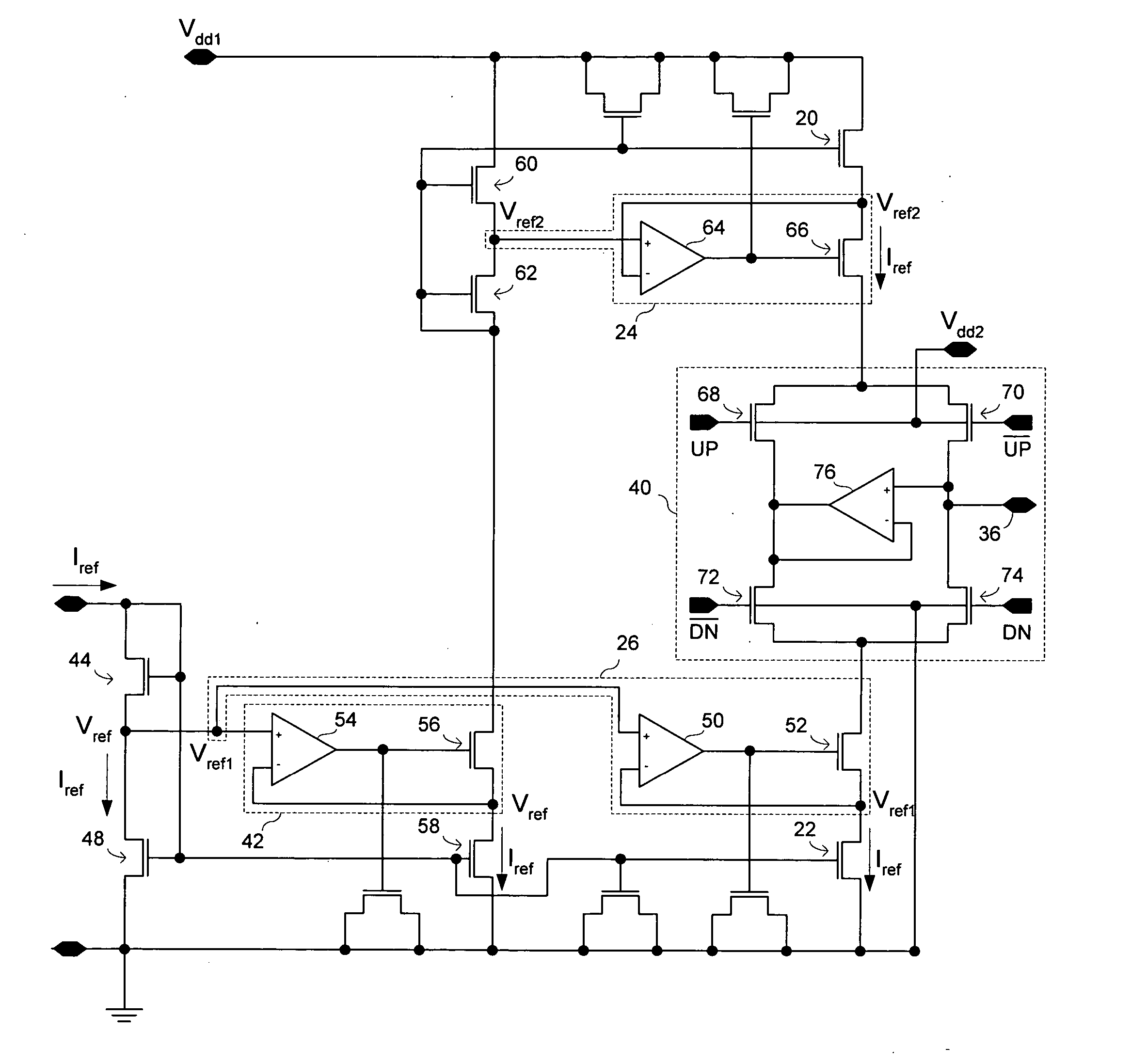
[0020] In accordance with preferred embodiments of the invention, a charge pump circuit uses active feedback control of current mirrors to provide matched current sources. The active feedback control is preferably implemented using voltage regulation devices that control the voltages that drive charge into and out of the charge pump output node. FIG. 5 shows a generalized schematic diagram of a charge pump circuit in accordance with preferred embodiments of the invention. The charge pump circuit utilizes MOSFETs as current source transistors 20, 22. Voltage regulation devices 24, 26 are placed in series with the current source transistors 20, 22 between the current source transistors 20, 22 and the switches 28, 30. The voltage regulation devices 24, 26 receive respective reference voltages Vref1, Vref2 at their inputs 32, 34 and control the drain voltages of the current source transistors 20, 22 so that the drain voltages are the same as the reference voltages. The values of the ref...


PUM


Abstract

A charge pump circuit utilizes active feedback control circuits to control the currents produced by sinking and sourcing current sources. The feedback control circuits may regulate the drain voltages of sinking and sourcing current source transistors to make them approximately equal to respective reference voltages received by the feedback control circuits. The charge pump circuit may utilize multiple supply voltages, with a higher supply voltage such as a 3.3 V supply voltage being used to drive current source transistors, and a lower supply voltage such as a 1.8 V supply voltage being used to drive switches in a switching section.

Description

BACKGROUND OF THE INVENTION [0001] 1. Field of the Invention [0002] Embodiments of the invention pertain to charge pump circuits and to circuits and devices incorporating charge pump circuits. [0003] 2. Related Technology [0004] Wireless communication devices typically require a frequency synthesis element to produce frequencies for modulating transmitted signals and demodulating received signals. Frequency synthesis is typically provided using a phase locked loop circuit. FIG. 1a shows an example of a conventional 3rd order phase locked loop, and FIG. 1b show an example of a conventional >3rd order phase locked loop. The phase locked loop is a feedback circuit comprised of a phase frequency detector 10, a charge pump 12, a low pass filter 14, a voltage controlled oscillator 16, and a frequency divider 18. The phase frequency detector 10 receives as inputs a reference frequency Fref and an output frequency Fout produced by the voltage controlled oscillator 16. The phase frequency...

Claims


Application Information

Patent Timeline
Patent Type & Authority Applications(United States)
IPC IPC(8): G05F1/10G05F3/02H02M3/18H02M7/25H03L7/00H03L7/06
CPCH03L7/0896
Inventor SOE, ZAW MIN
Owner REALTEK SEMICON CORP
Why Eureka
Try Eureka