Image sensor, optical pointing device and motion calculating method of optical pointing device

Inactive Publication Date: 2005-09-15
ATLAB INC
View PDF7 Cites 13 Cited by
  • Summary
  • Abstract
  • Description
  • Claims
  • Application Information

AI Technical Summary

Benefits of technology

[0021] The present invention, therefore, solves aforementioned problems associated with conventional devices by providing an image sensor which can obtain

Problems solved by technology

This may cause inconvenience to the user when the user uses a computer in a limited area such as a train

Method used


Image

  • Image sensor, optical pointing device and motion calculating method of optical pointing device
  • Image sensor, optical pointing device and motion calculating method of optical pointing device
  • Image sensor, optical pointing device and motion calculating method of optical pointing device

Examples


first embodiment

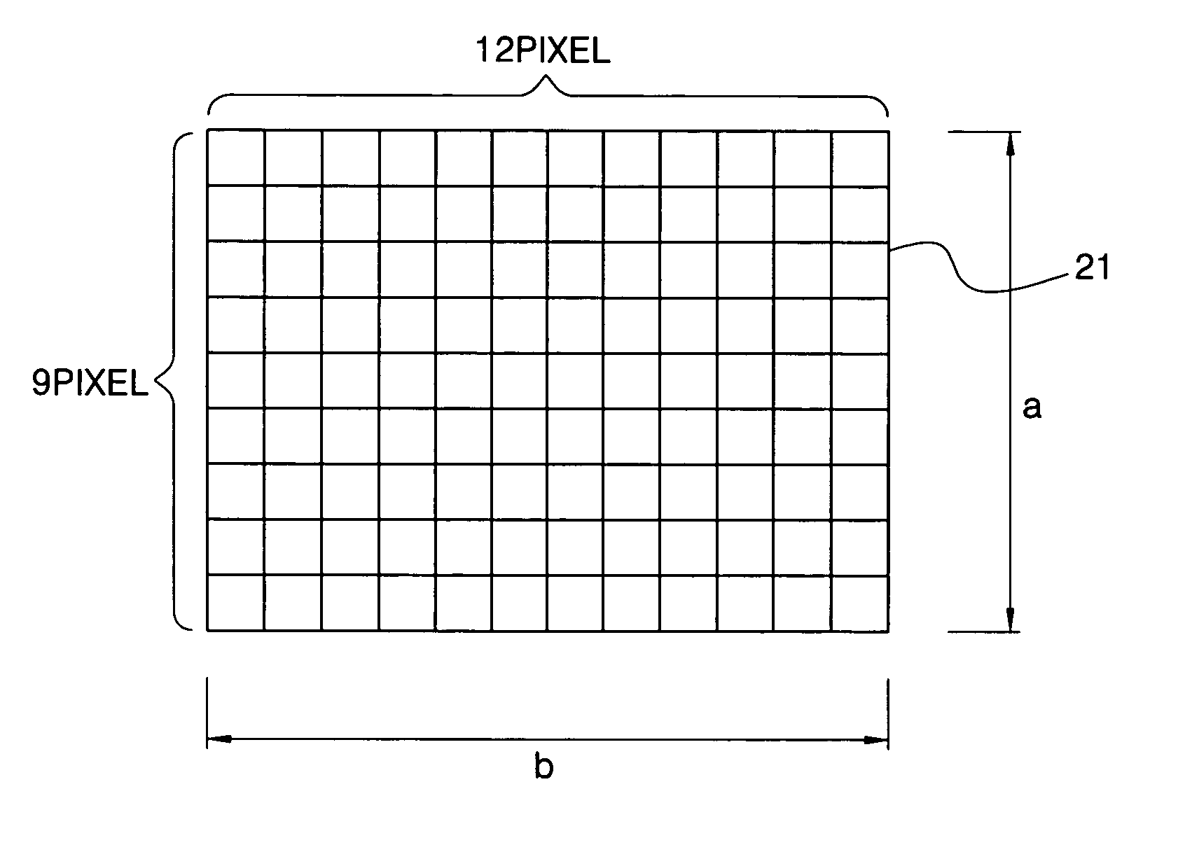
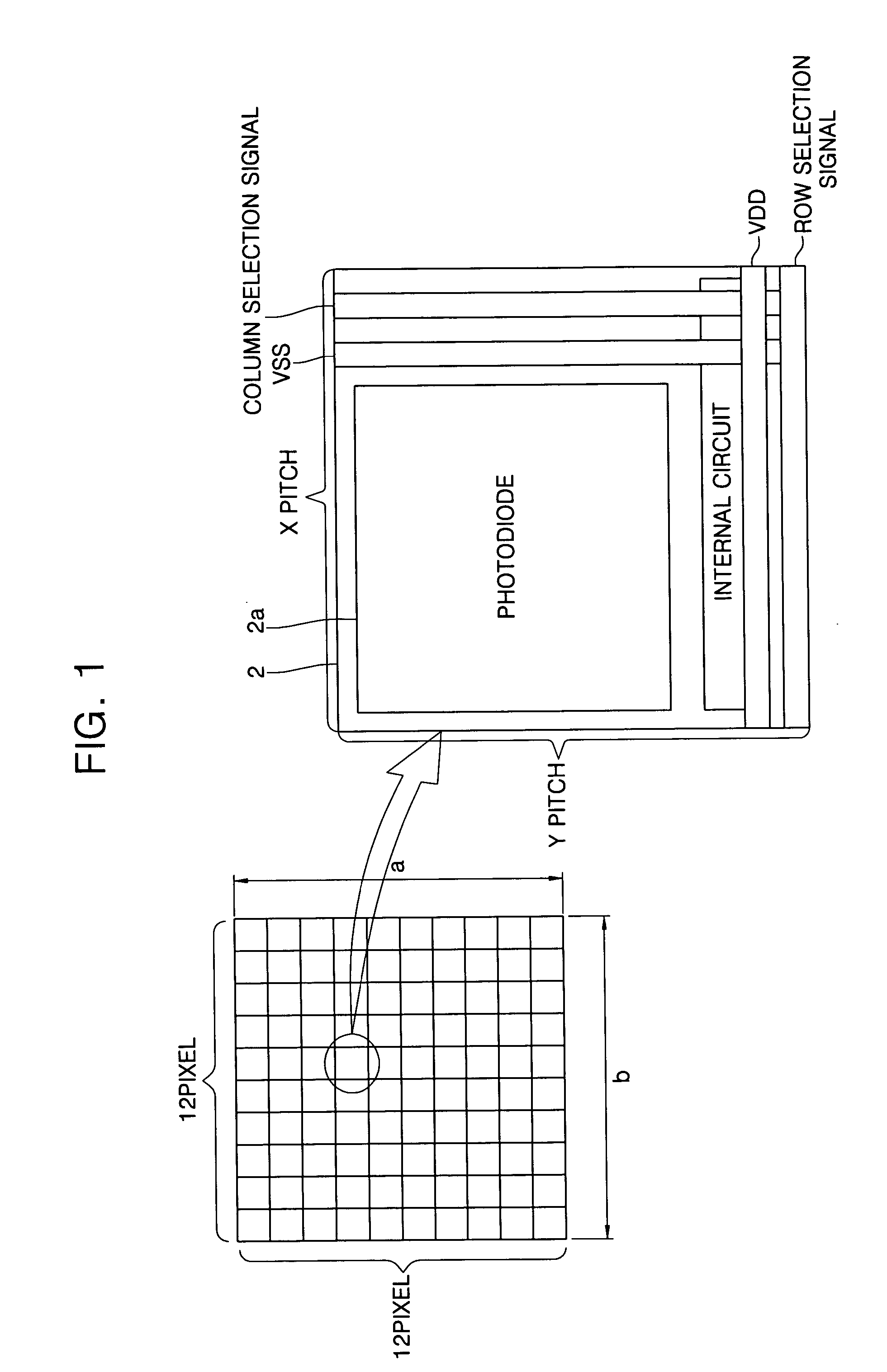
[0042]FIG. 4 is a schematic view of an image sensor according to the present invention.

[0043] As shown in FIG. 4, the image sensor 21 includes a pixel array in which the number (12) of pixels which forms an X axis is greater than the number (9 ) of pixels which forms a Y axis. Here, in each pixel, X and Y pitches have the same value like FIG. 1.

[0044] The image sensor 21 obtains a surface image that “b” of the X axis is longer than length “a” of the Y axis while the shutter thereof is in an ON state, and outputs 12 ×9 electrical signals corresponding to each of the obtained surface image areas to an internal circuit of an optical pointing device.

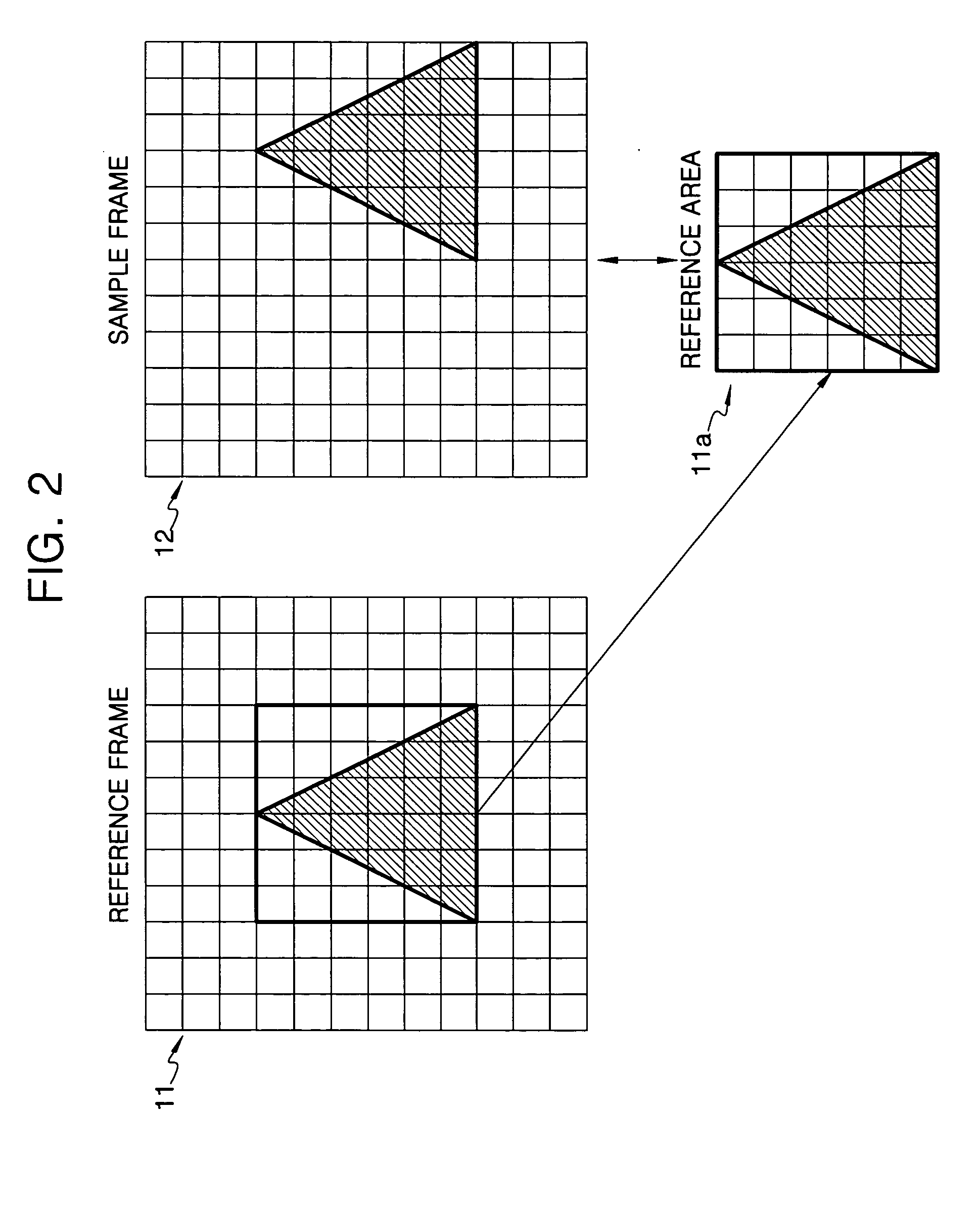
[0045]FIG. 5 is a schematic view illustrating a motion calculation method of an optical pointing device which employs the image sensor of FIG. 4.

[0046] In FIG. 5, a frame 31 has an image of a surface obtained through the image sensor of FIG. 4 during a previous sampling period, and a frame 32 has an image of a surface obtained during a cu...

second embodiment

[0053]FIG. 6 is a schematic view of an image sensor according to the present invention.

[0054] As shown in FIG. 6, the image sensor 41 is configured such that the X-axis length “b” is identical to the Y-axis length “a” but the X axis is smaller in pitch than the Y axis. The number (12 ) of pixels which form the X axis is greater than the number (9) of pixels which form the Y axis.

[0055] As described above, using the image sensor of FIG. 6, a resolution for the motion of the optical pointing device for the X axis direction is increased, and so even though it moves the same distance in X axis and Y axis directions respectively, the motion value for the X axis direction sensed by the optical pointing device is greater than that for the Y axis direction.

[0056] Also, an actual motion distance of the optical pointing device is smaller than a calculated motion distance.

[0057] That is, in case of moving a cursor on a monitor screen which represents a motion value of the optical pointing d...


PUM


Abstract

An image sensor, an optical pointing device and a motion calculating method of the optical pointing device are disclosed. The optical pointing device includes an image sensor for obtaining and providing a surface image corresponding to a motion searching range; and an image processor for determining a direction and a length of an X axis and a Y axis of the motion searching range and a reference area to continuously obtain the surface image corresponding to the direction and length of the X axis and Y axis, obtaining a reference frame and a current frame using the continuously obtained surface image, setting a certain area of the reference frame corresponding to the direction and length of the X axis and Y axis of the reference area as the reference area, and calculating a correlation between the reference area and the sample frame, to thereby calculate motion. The image sensor can obtain the larger surface image in the X axis direction. Thus, even though the optical pointing device collects the image at a low sampling rate, there is an effect in that larger motion of the optical pointing device for the X axis direction can be calculated. This helps reduce the operating speed of the semiconductor to thereby reduce power consumption.

Description

CROSS-REFERENCE TO RELATED APPLICATION [0001] This application claims priority to and the benefit of Korean Patent Application No. 2004-16607 , filed Mar. 11, 2004, the disclosure of which is incorporated herein by reference in its entirety.BACKGROUND OF THE INVENTION [0002] 1. Field of the Invention [0003] The present invention relates to an optical pointing device and, more particularly, to an image sensor, an optical pointing device and a motion calculating method of the optical pointing device which can calculate larger motion of the optical pointing device for an X axis direction. [0004] 2. Description of the Related Art [0005] In general, an image sensor gets a surface image and provides an image processing device with the surface image. The image processing device which employs the image sensor includes, for example, a digital camera and an optical pointing device. [0006] The field in which the present invention concerns is an image sensor which is employed in an optical poin...

Claims


Application Information

Patent Timeline
IPC IPC(8): G06F3/033G06F3/03G09G5/00
CPCG06F3/0317G06T2207/10016G06T7/204G06T7/248A61P31/04E05B65/025E05B65/44
Inventor LEE, BANG-WON
Owner ATLAB INC
Why Eureka
Try Eureka