Delay circuit

a delay circuit and circuit technology, applied in the field of delay circuits, can solve the problems of reducing the accuracy of record recording, unable to record desired record marks, etc., and achieve the effects of preventing the reduction of accuracy, doubling the accuracy of recording on a disk, and high-speed recording

Active Publication Date: 2005-09-22
SEMICON COMPONENTS IND LLC
View PDF11 Cites 8 Cited by
  • Summary
  • Abstract
  • Description
  • Claims
  • Application Information

AI Technical Summary

Benefits of technology

[0012] Hence, it is an object of the present invention to provide a delay circuit that can double

Problems solved by technology

However, because the record state varies depending on the type of medium to record data thereon and on the rotation speed of the disk, desired record marks cannot be recorded by simply

Method used


Image

  • Delay circuit
  • Delay circuit
  • Delay circuit

Examples


embodiment 1

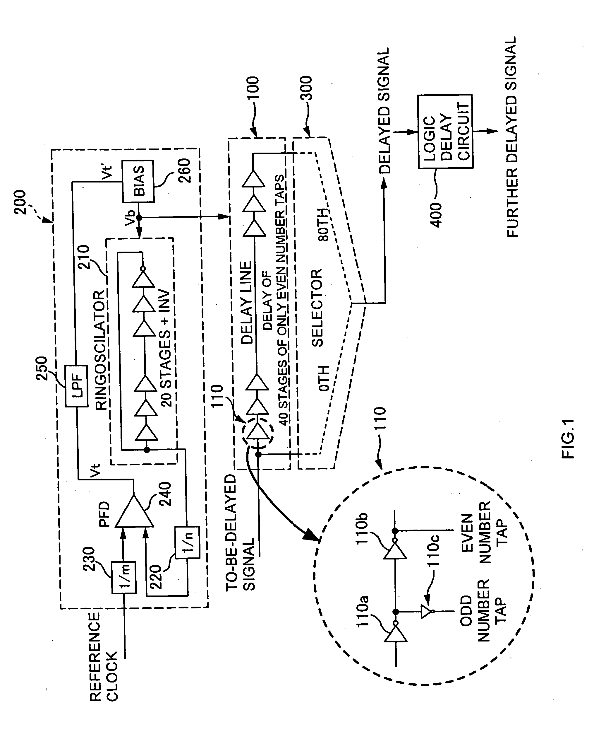
[0030] A delay circuit according to an embodiment of the present invention will be described with reference to FIG. 1.

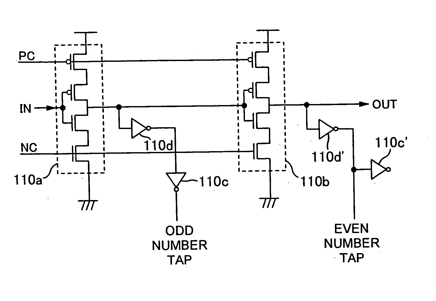
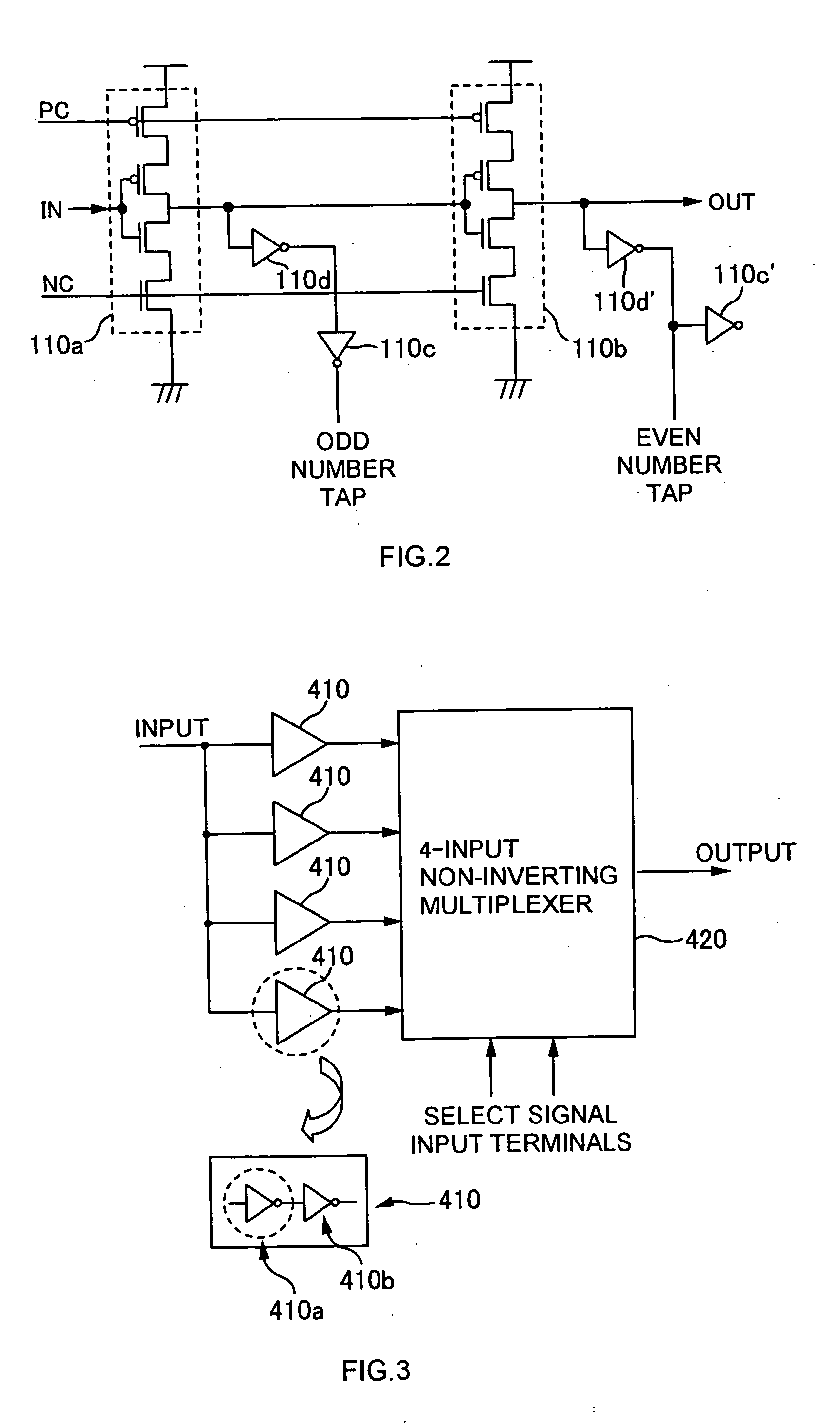
[0031] As shown in the Figure, the delay circuit comprises a delay line 100 that delays its input signal as a to-be-delayed signal, a PLL circuit 200 that controls the delay amount of this delay line, and a first selector 300 that selects from the output signals from the delay line 100. The PLL circuit 200 supplies the delay line 100 with a control voltage (delay control voltage) Vb to control the delay amount of the delay line 100. The delay line 100 has 40 delay cells 110 connected in series. Each delay cell 110 has two stages of delay inverters 110a, 110b connected in series and an output inverter 110c. The input terminal of the output inverter 110c is connected to the connection point of the delay inverter 110a at the first stage and the delay inverter 110b at the second stage. In the delay cell 110, the output signal from the delay inverter 110b at the second s...

embodiment 2

[0038] Embodiment 2 that is a further improvement over the delay circuit of embodiment 1 will be described. As shown in FIG. 1, the delay circuit further comprises a logic delay circuit (signal delaying section) 400. This logic delay circuit further delays the delayed signal output from the first selector 300 and outputs the further delayed signal. With this configuration, the delay can be controlled independently without being restricted by control voltage Vb supplied from the PLL circuit 200 to the delay line at the preceding stage of the first selector 300.

[0039] The specific configuration of the logic delay circuit 400 includes a plurality (e.g. four) of buffer circuits 410 having the delayed signal from the first selector 300 inputted thereto and a non-inverting multiplexer (second selector) 420 with a plurality (the same number as that of the buffer circuits, e.g. four) of inputs. The buffer circuits 410 are connected in parallel and configured to differ in delay amount from ...


PUM


Abstract

A delay circuit comprising a delay line to delay an input signal that has a plurality of delay cells connected in series; a PLL circuit that supplies the delay line with a delay control voltage to control the delay; and a first selector that selects one of output signals of the delay cells. Each of the delay cells comprises two stages of delay inverters connected in series and an output inverter connected to a connection point of the delay inverter of the first stage and the delay inverter of the second stage. Input into the delay inverter of the first stage is an output signal of the delay inverter of the second stage in the preceding delay cell, and the first selector outputs as a delayed signal an output signal of the output inverter or the delay inverter of the second stage in one of the delay cells.

Description

CROSS-REFERENCE TO RELATED APPLICATIONS [0001] The present application claims priority upon Japanese Patent Application No. 2004-077636 filed on Mar. 18, 2004, which is herein incorporated by reference. BACKGROUND OF THE INVENTION [0002] 1. Field of the Invention [0003] The present invention relates to a delay circuit for preventing the reduction in recording accuracy at high speed recording on a disk. [0004] 2. Description of the Related Art [0005] Data-recordable optical disk apparatuses and magneto optical disk apparatuses write data onto a disk by recording record marks corresponding to a data modulated signal on the disk with a laser. For example, for CD-Rs, first, data to be recorded is modulated into an EFM signal in an EFM encoder, and this EFM signal is sent to a laser apparatus, and then record marks corresponding to the EFM signal are recorded on a disk. [0006] However, because the record state varies depending on the type of medium to record data thereon and on the rotat...

Claims


Application Information

Patent Timeline
IPC IPC(8): G11B20/10G11B7/00G11B20/14H03H11/26H03K5/00H03K5/14H03L7/00
CPCH03H11/265H03K2005/00104H03K5/133
Inventor SHUTOKU, TOSHIYUKIHAYASHI, KOJI
Owner SEMICON COMPONENTS IND LLC
Why Eureka
Try Eureka