Electrostatic discharge protection device and method therefore

a protection device and electrostatic discharge technology, applied in semiconductor devices, semiconductor/solid-state device details, transistors, etc., can solve the problems of esd devices being disabled during normal operation of integrated circuits, circuitry of integrated circuits that couples to i/o can be damaged, and integrated circuits are prone to electrostatic discharge (esd)

Active Publication Date: 2005-09-22
MOTOROLA INC
View PDF3 Cites 38 Cited by
  • Summary
  • Abstract
  • Description
  • Claims
  • Application Information

AI Technical Summary

Problems solved by technology

An integrated circuit is prone to damage by electrostatic discharge (ESD) throughout its life cycle, from manufacture to use in a product.
An electrostatic discharge event is a high energy impulse having a voltage amplitude typically measuring thousands of volts that can physically and permanently damage a semiconductor device.
The circuitry of the integrated circuit that couples to an I/O can be damaged unless protected by an electrostatic discharge protection circuit or device.
ESD protection of an integrated circuit has always been a critical issue as the semiconductor industry continues the trend of shrinking transistor geometries to maxim

Method used


Image

  • Electrostatic discharge protection device and method therefore
  • Electrostatic discharge protection device and method therefore
  • Electrostatic discharge protection device and method therefore

Examples


Embodiment Construction

[0024] The following detailed description is merely exemplary in nature and is not intended to limit the invention or the application and uses of the invention. Furthermore, there is no intention to be bound by any expressed or implied theory presented in the preceding technical field, background, brief summary or the following detailed description.

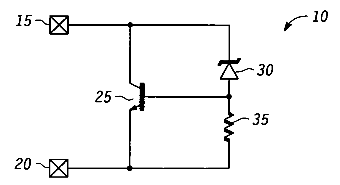
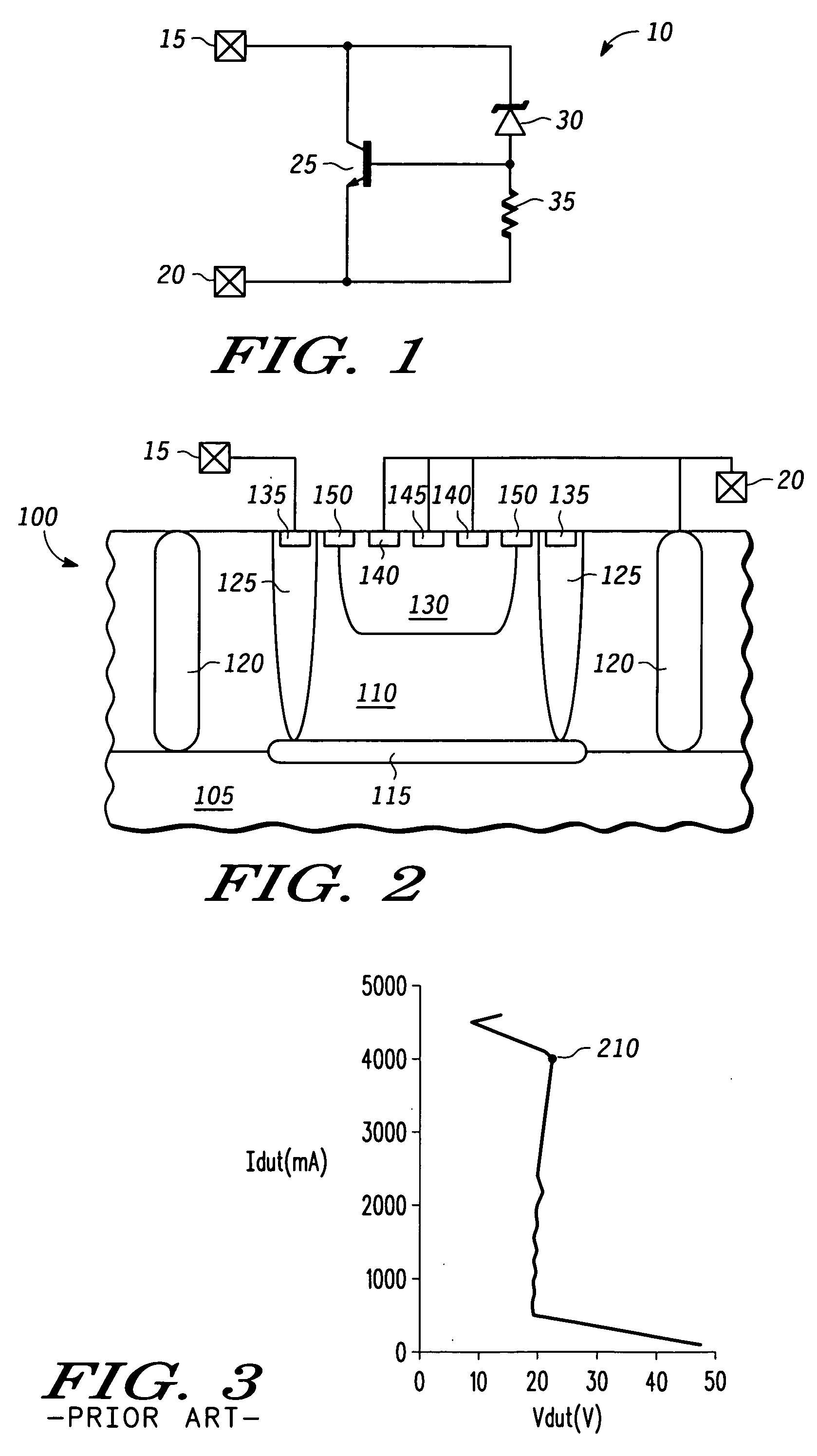
[0025] A zener diode triggered bipolar transistor electrostatic discharge (ESD) protection circuit similar to that shown in FIG. 1 is capable of being formed on both existing and future wafer process flows. In general, cost is a factor in the design of an ESD protection circuit. Typically, an electrostatic discharge protection circuit is made from process steps and masks that exist in the wafer flow. The use of extra mask or wafer process steps to optimize performance of the ESD protection circuit performance is rarely justified due to the increased cost of manufacture. Another variable affecting the cost of ESD protection circuit is the...


PUM


Abstract

Methods and apparatus are provided an electrostatic discharge (ESD) protection device having a first terminal and a second terminal. The ESD protection device comprises a vertical transistor having a collector coupled to the first terminal, a base, and an emitter coupled to the second terminal. A zener diode has a first terminal coupled to the first terminal of the ESD protection device and a second terminal coupled to the base of the vertical transistor. Subsurface current paths are provided to redistribute current from a surface of the vertical transistor in an ESD event. The method comprises generating an ionization current when a zener diode breaks down during an ESD event. The ionization current density from a surface zener diode region is reduced. The ionization current enables a transistor to dissipate the ESD event.

Description

TECHNICAL FIELD OF THE INVENTION [0001] The present invention generally relates to electrostatic discharge protection, and more particularly relates to an electrostatic discharge structure having a zener diode triggered bipolar transistor. BACKGROUND OF THE INVENTION [0002] An integrated circuit is prone to damage by electrostatic discharge (ESD) throughout its life cycle, from manufacture to use in a product. An electrostatic discharge event is a high energy impulse having a voltage amplitude typically measuring thousands of volts that can physically and permanently damage a semiconductor device. In general, an electrostatic discharge event is coupled to circuitry of an integrated circuit through the input / output (I / O) of the device. The I / O are the interface of the integrated circuit for receiving / sending signals from off chip. The circuitry of the integrated circuit that couples to an I / O can be damaged unless protected by an electrostatic discharge protection circuit or device. ...

Claims


Application Information

Patent Timeline
IPC IPC(8): H01L27/02H01L29/732H02H9/00
CPCH01L29/7322H01L27/0259
Inventor XU, HONGZHONGBAUMERT, BETH A.IDA, RICHARD T.
Owner MOTOROLA INC
Why Eureka
Try Eureka