High frequency circuit block unit, method for producing same, high frequency module device and method for producing same

a high frequency circuit and block unit technology, applied in the direction of printed circuit non-printed electric components, high frequency circuit adaptations, waveguides, etc., can solve the problems of increasing the overall power consumption, difficult to achieve a sufficient gain, and insufficient characteristics of conventional high frequency transmission/reception circuits to meet required specifications

Inactive Publication Date: 2005-09-22
SONY CORP
View PDF1 Cites 21 Cited by
  • Summary
  • Abstract
  • Description
  • Claims
  • Application Information

AI Technical Summary

Benefits of technology

[0032] It is therefore an object of the present invention to provide a high frequency circuit block unit, a producing method therefor, a high frequency module device and a producing method therefor, by means of which the problems inherent in the conventional high frequency module device may be overcome.
[0033] It is another object of the present invention to provide a high frequency circuit block unit, a producing method therefor, a high frequency module device and a producing method therefor, by means of which passive devices or the wiring unit can be formed with high precision and the unit or device may be reduced in size and cost.
[0035] In this high frequency circuit block unit, the major surfaces of the plural unit wiring layers are planarized in their entirety, and the dummy substrate is removed to produce the block unit. Thus, the major surfaces of the respective unit wiring layers are not susceptible to micro-irregularities, so that the passive devices and the wiring layers may be formed on the respective unit wiring layers with high precision. Since the base substrate is unneeded, the block unit may be reduced in size and cost.
[0037] In this method for producing a high frequency circuit block unit, plural unit wiring layers, each made up by an insulating layer and a wiring layer, are formed on a dummy substrate, the major surfaces of the respective unit wiring layers are planarized in their entirety and the dummy substrate is removed from the plural unit wiring layers to produce the high frequency circuit block unit. Thus, in the present method for producing a high frequency circuit block unit, the major surfaces of the respective unit wiring layers are not susceptible to micro-irregularities, so that the passive devices and the wiring layers may be formed on the respective unit wiring layers with high precision. Since the base substrate is unneeded, the block unit produced may be reduced in size and cost.
[0039] In this high frequency module device, the major surfaces of the plural unit wiring layers, making up the high frequency circuit block unit, layered on the dummy substrate, are planarized in their entirety, and the dummy substrate is removed to produce the high frequency circuit block unit. Thus, in the high frequency module device, the major surfaces of the respective unit wiring layers of the high frequency circuit block unit are not susceptible to micro-irregularities, so that the passive devices and the wiring layers may be formed on the respective unit wiring layers with high precision. Since the base substrate is unneeded, the block unit produced may be reduced in size and cost.
[0041] In this producing method for a high frequency module device, a plural number of unit wiring layers, each made up by an insulating layer and a wiring layer, are formed on a dummy substrate, the major surfaces of the unit wiring layers are planarized, and the dummy substrate is removed from the plural unit wiring layers to form a high frequency circuit block unit, which is mounted on the motherboard to produce the high re module device. Thus, with the present producing method for a high frequency module device, the major surfaces of the respective unit wiring layers of the high frequency circuit block unit are not susceptible to micro-irregularities, so that the passive devices and the wiring layers may be formed on the respective unit wiring layers with high precision. Since the base substrate is unneeded, the block unit produced may be reduced in size and cost.

Problems solved by technology

In the high frequency transmission / reception circuit 110, since the signals are amplified at a time in a high frequency stage, it becomes difficult to achieve a sufficient gain, so that the amplifying operation needs to be performed in the baseband unit.
Thus, the high frequency transmission / reception circuit 110 is in need of a circuit for canceling DC offset, or redundant low-pass filters, thus further increasing the overall power consumption.
The conventional high frequency transmission / reception circuit is not of sufficient characteristics to satisfy required specifications, such as reduction in size or weight of the communication terminal equipment, whether the circuit is of the superheterodyne type or the direct conversion type.
This high frequency circuit substrate suffers a problem that the inductor unit 120 has to be formed by numerous cumbersome process steps, thus raising the cost.
Moreover, in the high frequency circuit substrate, the electrical interference between the high frequency circuit section of the analog circuit and the baseband circuit section of the digital circuit poses a serious problem.
Thus, in the high frequency circuit substrates 130, 140, such problems may be produced as electrical interference across respective wirings, increased cost due to multi-layered wirings or bulkiness in size due to layout of the interconnections.

Method used


Image

  • High frequency circuit block unit, method for producing same, high frequency module device and method for producing same
  • High frequency circuit block unit, method for producing same, high frequency module device and method for producing same
  • High frequency circuit block unit, method for producing same, high frequency module device and method for producing same

Examples


Embodiment Construction

[0075] Referring to the drawings, certain preferred embodiments of the present invention will be explained in detail.

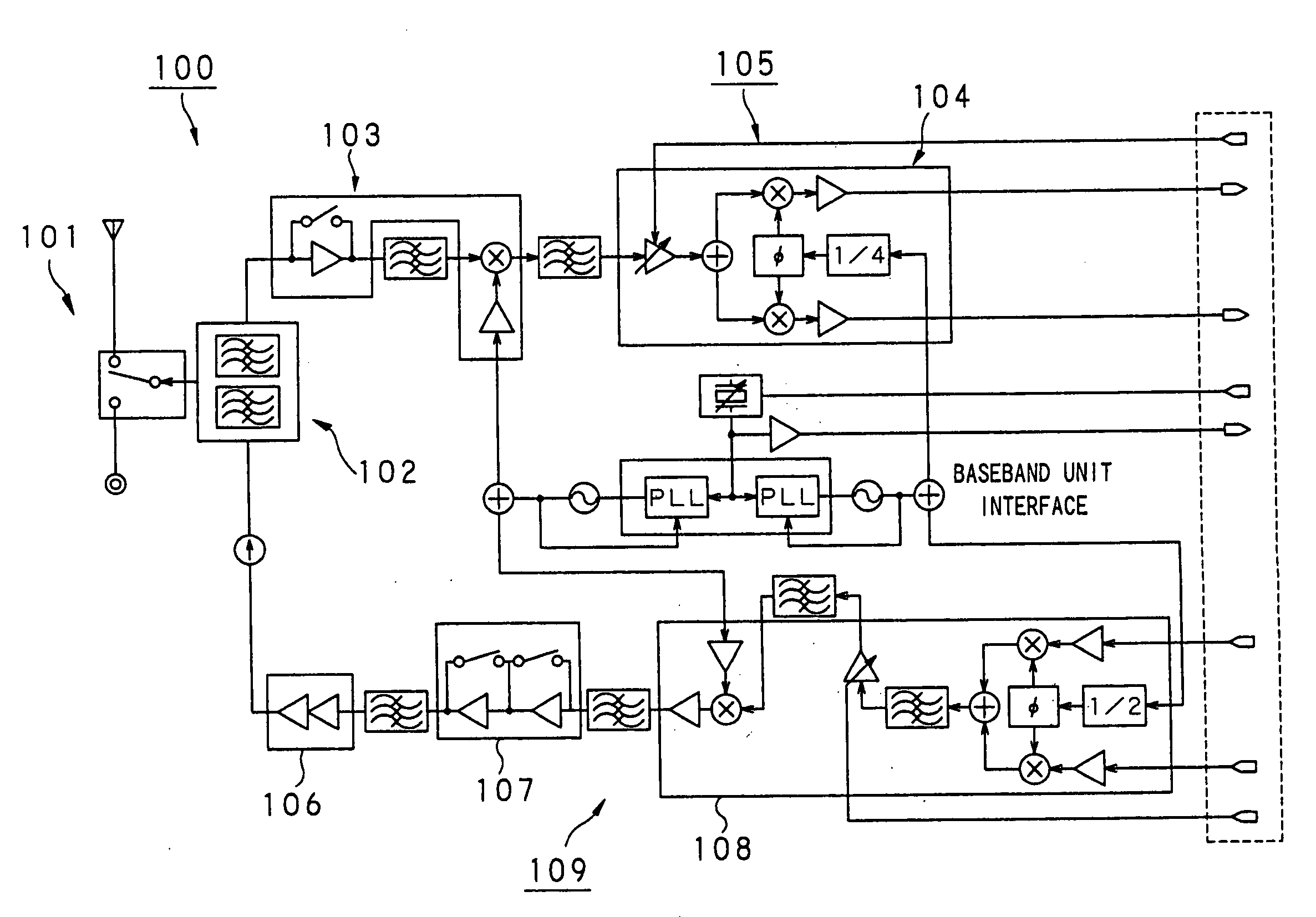
[0076] A high frequency module device 1 according to the present invention forms a high frequency circuit for performing exchange operations, etc. for high frequency signals by, for example, a superheterodyne system or a direct conversion system, in a transmission / reception unit provided in e.g., a portable communication terminal equipment, as shown in FIG. 7. The high frequency module device 1 is comprised of a high frequency circuit block unit 2, hereinafter referred to as a block unit, that is a high frequency circuit substrate, electrically connected and mounted to a motherboard 3 by for example bump units 4, such as solder.

[0077] The block unit 2 includes a second unit wiring layer 6, layered on the major surface of a first unit wiring layer 5, and a third unit wiring layer 7 on the major surface of the second unit wiring layer 6. These first to third unit wiri...


PUM


Abstract

A high frequency module device having a high frequency circuit block unit including a passive device. A plural number of unit wiring layers, each formed by an insulating layer, having a passive device unit in its portion, and by a pattern wiring, are layered on a dummy substrate, and are released from the dummy substrate to form the high frequency circuit block unit (2), which is mounted on a motherboard (3). The major surfaces of the respective unit wiring layers are planarized. The passive device unit and the pattern wiring, formed on the major surface of each unit wiring layer in the high frequency circuit block unit (2), can be formed with high accuracy to improve high frequency characteristics. The high frequency circuit block unit (2) is not in need of a base substrate, thus achieves reduction in size and cost.

Description

TECHNICAL FIELD [0001] This invention relates to a high frequency circuit block unit, having a passive device, a manufacturing method therefor, a high frequency module device having the high frequency circuit block unit mounted on a motherboard, and a manufacturing method therefor. [0002] This application claims priority of Japanese Patent: Application No. 2001-359853, filed on Nov. 26, 2001, the entirety of which is incorporated by reference herein. BACKGROUND ART [0003] A variety of the information, such as audio or video information, is converted into digital signals and handled as digital data, and hence may readily be handled by for example a personal computer or by a mobile computer. The above information may be compressed in bandwidth by an audio codec or video codec technology so as to be distributed by digital communication or digital broadcast to a variety of communication terminal equipment readily efficiently. For example, audio / video data (AV data) may be received outdo...

Claims


Application Information

Patent Timeline
Patent Type & Authority Applications(United States)
IPC IPC(8): H05K1/16H01L21/48H01L21/60H01L21/68H01L23/498H01L23/552H01L23/66H01L25/00H01P3/02H04B1/40H04B1/52H05K1/02H05K1/14H05K1/18H05K3/00H05K3/26H05K3/28H05K3/46
CPCH01L21/4857H01L2224/16225H01L23/49822H01L23/552H01L23/66H01L24/81H01L2221/68345H01L2221/68359H01L2221/68363H01L2224/16H01L2224/73253H01L2224/81801H01L2924/01013H01L2924/01029H01L2924/01033H01L2924/01038H01L2924/01056H01L2924/01073H01L2924/01078H01L2924/01079H01L2924/01082H01L2924/09701H01L2924/14H01L2924/16152H01L2924/19041H01L2924/19042H01L2924/19043H01L2924/19105H01L2924/19107H01L2924/30105H01L2924/30107H01L2924/3025H04B1/52H05K1/0237H05K1/141H05K1/16H05K3/007H05K3/4614H05K3/4644H05K3/4682H05K3/4694H05K2201/0352H05K2201/09972H05K2203/016H05K2203/061H01L2924/01005H01L2924/01006H01L2924/01024H01L2924/01075H01L2924/01076H01L2924/014H01L21/6835H01L2224/32245H01L2924/00014H01L2924/12042H01L2924/00H01L2224/0401H05K1/11
Inventor OGAWA, TSUYOSHI
Owner SONY CORP
Why Eureka
Try Eureka