Field effect transistor

a field-effect transistor and transistor technology, applied in transistors, semiconductor devices, electrical equipment, etc., can solve the problems of large driving current, difficult to satisfy this requirement by a diffused layer of impurities, and large driving current provided

Inactive Publication Date: 2005-09-29
KK TOSHIBA
View PDF3 Cites 20 Cited by
  • Summary
  • Abstract
  • Description
  • Claims
  • Application Information

AI Technical Summary

Benefits of technology

[0019]FIG. 10 shows a sectional view of a MIS type field effect transistor concerning the fifth embodiment;
[0020]FIG. 11 shows a perspective view of a MIS type field effect transistor concerning the sixth embodiment; and
[0021]FIGS. 12A and 12B show sectional views of a MIS type field effect transistor concerning the sixth embodiment.

Problems solved by technology

It is difficult to satisfy this requirement by an impurity diffused layer.
However, in the MOSFET of this kind of Schottky source / drain structure, there is a problem that a large driving current is not provided due to a contact resistance caused by a Schottky barrier formed at an interface between a metal source / drain and a channel semiconductor.
There is a problem that a large driving current is not provided due to a contact resistance caused by a Schottky barrier in this device, too.
However, this kind of transistor has a problem that a large driving current is not provided due to an increase of a contact resistance caused by a Schottky barrier.

Method used


Image

  • Field effect transistor
  • Field effect transistor
  • Field effect transistor

Examples


first embodiment

[0023] (First Embodiment)

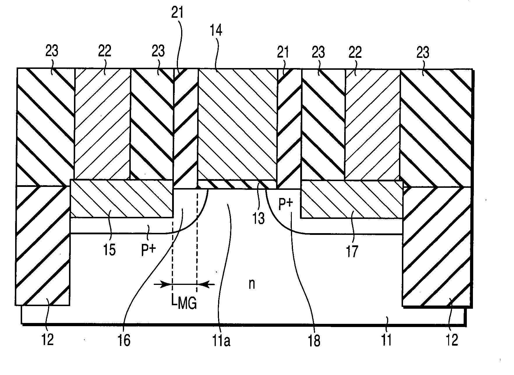
[0024]FIG. 1 shows a sectional view of a field effect transistor concerning the first embodiment of the present invention. This transistor is a p-channel MOSFET of a Schottky source / drain structure having an additional diffused layer, the gate length is assumed 20 nm.

[0025] A device separation insulating film 12 is formed of a Si oxide film, and so on, and buried in an n type Si substrate (first semiconductor region) 11. A gate electrode 14 is formed on a channel region 11a in a device formation region surrounded by the device separation insulating film 12 with a gate insulating film 13 interposed between the channel region 11a and the gate electrode 14. A source electrode 15 and a drain electrode 17 configuring Schottky source and drain are formed in the device formation region with the channel region 11a arranged between the source and drain electrodes 15 and 17. The gate electrode 14 and the source and drain electrodes 15 and 17 are made of platinum sili...

second embodiment

[0050] (Second Embodiment)

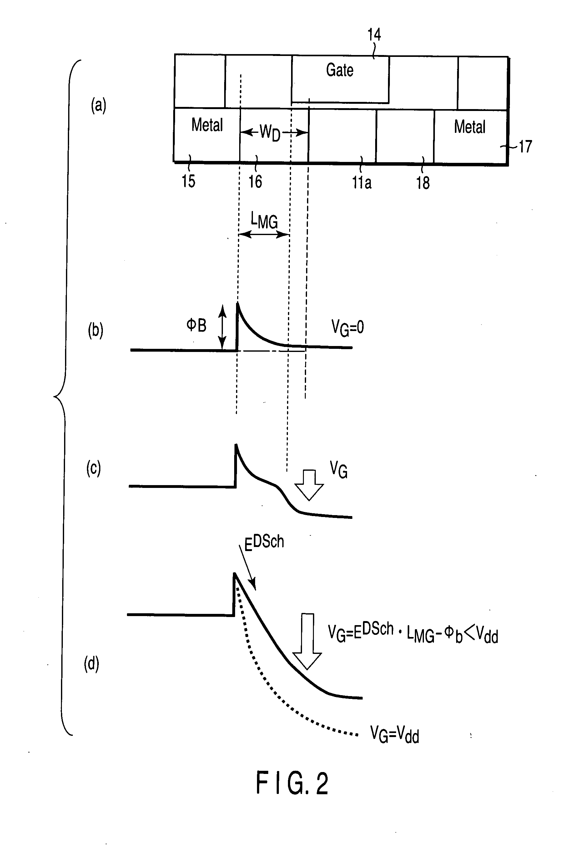
[0051] There will be explained a method of setting a tolerance of a distance LMG between the gate electrode 14 and the source electrode 15 in the MOSFET shown in FIG. 1 as the second embodiment of the present invention.

[0052]FIG. 3 shows a graph for obtaining the tolerance of the distance LMG between the gate electrode 14 and the source electrode 15 according to Schottky barrier height. The horizontal axis shows the impurity concentration of the additional diffused layer 16, and the vertical axis shows the distance LMG.

[0053] The MOSFET of the present embodiment can use an additional diffused layer concentration higher than that of the first embodiment as seen from the graph of FIG. 3. Then, since the maximum electric field of Schottky barrier increases, it is necessary to approximate the source electrode 15 to the gate electrode 14 in order to control the Schottky barrier width with the electric field of the gate.

[0054] In the graph of FIG. 3, in the ca...

third embodiment

[0070] (Third embodiment)

[0071] The third embodiment of the present invention will be described on a method of manufacturing a MOSFET of FIG. 1 referring to FIGS. 5A to 5D.

[0072] A device separation insulating film 12 is buried in a device isolating region of an n type Si substrate 11 by a known method as shown in FIG. 5(a). After formation of a sacrifice oxide film of around 5 nm, a channel impurity for controlling a threshold voltage is introduced in the substrate by an ion implantation (not shown).

[0073] After exfoliation of the sacrifice oxide film, a gate insulator 13 of an effective oxide film thickness around 1 nm is formed on the substrate 11. A gate electrode 14 is formed by a method of lithography. Subsequently, a TEOS film for forming an offset spacer is deposited on the gate electrode and the substrate, and an offset spacer 25 is formed around the gate electrode 14 by a side wall remaining method using anisotropic etching.

[0074] An ion implantation is done by BF2 of, ...


PUM


Abstract

An field effect transistor includes a first semiconductor region, a gate electrode insulatively disposed over the first semiconductor region, source and drain electrodes between which the first semiconductor region is sandwiched, and second semiconductor regions each formed between the first semiconductor region and one of the source and drain electrodes, and having impurity concentration higher than that of the first semiconductor region, the source electrode being offset to the gate electrode in a direction in which the source electrode and the drain electrode are separated from each other with respect to a channel direction, and one of the second semiconductor regions having a thickness not more than a thickness with which the one of second semiconductor regions is completely depleted in the channel direction being in thermal equilibrium with the source electrode therewith.

Description

CROSS-REFERENCE TO RELATED APPLICATIONS [0001] This application is based upon and claims the benefit of priority from prior Japanese Patent Application No. 2004-092537, filed Mar. 26, 2004, the entire contents of which are incorporated herein by reference. BACKGROUND OF THE INVENTION [0002] 1. Field of the Invention [0003] The invention relates to a MIS (Metal Insulator Semiconductor) type field effect transistor configuring a semiconductor integrated circuit, and particularly to a MIS type field effect transistor, which is improved in source and drain. [0004] 2. Description of the Related Art [0005] High performance of a field effect transistor has been achieved by microminiaturization on the basis of a scaling rule. However, in the field effect transistor whose gate length is not more than 15 nm, the source and drain whose thickness is as shallow as 10 nm and whose resistance is as low as 700 Ω are required. It is difficult to satisfy this requirement by an impurity diffused layer...

Claims


Application Information

Patent Timeline
Patent Type & Authority Applications(United States)
IPC IPC(8): H01L29/417H01L21/00H01L21/336H01L29/76H01L29/772H01L29/78H01L29/786
CPCH01L29/66643H01L29/66795H01L29/78621H01L29/785H01L29/7839
Inventor NAKABAYASHI, YUKIONISHINOHARA, KAZUMIKINOSHITA, ATSUHIROKOGA, JUNJI
Owner KK TOSHIBA
Why Eureka
Try Eureka