Electron emission element

a technology of electron emission element and element, which is applied in the direction of discharge tube/lamp details, discharge tube luminescnet screen, discharge tube main electrode, etc., can solve the problems of complicated driving mechanism, inability to simple configuration of apparatus including electron emission element and the like, and inability to manufacture simple driving mechanism, etc., to achieve simple manufacturing, increase the degree of freedom of displacement of electron emission unit, and low cost

Inactive Publication Date: 2005-09-29
PIONEER CORP
View PDF2 Cites 30 Cited by
  • Summary
  • Abstract
  • Description
  • Claims
  • Application Information

AI Technical Summary

Benefits of technology

[0009] The above-mentioned electron emission element makes the cathode substrate function as a cathode, and applies the voltage to the cathode and an anode. Thereby the electron emission element emits the electron from the electron emission unit provided on the cathode substrate, and irradiates the electron on the electron irradiation surface formed on the anode surface. The electron emission unit may be the electron source for example, and is thread-type and provided on the cathode substrate. The deflection unit generates the electric field around the electron emission unit. Since the electron emission unit has a charge, it receives a power from the generated electric field. Thereby, the thread-type electron emission unit is deflected to curve, and its tip from which the electron is emitted is moved. Therefore, the position on the electron irradiation surface (hereinafter referred to as “irradiation position”) at which the electron from the electron emission unit is irradiated is moved on the electron irradiation surface. Thereby, since it becomes unnecessary to move the electron irradiation surface onto which the electron is irradiated and the position of the entire electron emission unit, the configuration of the electron emission element or the apparatus including the electron emission element can be simple, not complicated.
[0014] In the embodiment, the electron emission unit is deflected by the two pairs of deflection electrodes (the first and second deflection electrodes) provided in the longitudinal direction of the electron emission unit. In this case, since the powers are applied to two portions of the electron emission unit being deflected, a degree of freedom of displacement of the electron emission unit increases. Namely, the distance between the tip of the electron emission unit and the electron irradiation surface can be adjusted. By applying the voltage suitable for the deflection electrodes, the distance between the tip of the electron emission unit and the electron irradiation surface can be maintained constant, and the electron emission unit can be deflected. Thus, the electron irradiation surface can be made plane. As a result, the electron emission element can be manufactured simply and at low cost.

Problems solved by technology

However, by the above-mentioned techniques, the mechanism of the apparatus including the electron emission element and the like sometimes becomes complicated, and a configuration thereof cannot be simple.
When the recording medium is moved, a complicated driving mechanism is necessary, for example.
When the cantilever is used, the mechanism for driving the cantilever similarly becomes complicated.
Therefore, the apparatus problematically becomes complicated and large.

Method used


Image

  • Electron emission element
  • Electron emission element
  • Electron emission element

Examples


first embodiment

[First Embodiment]

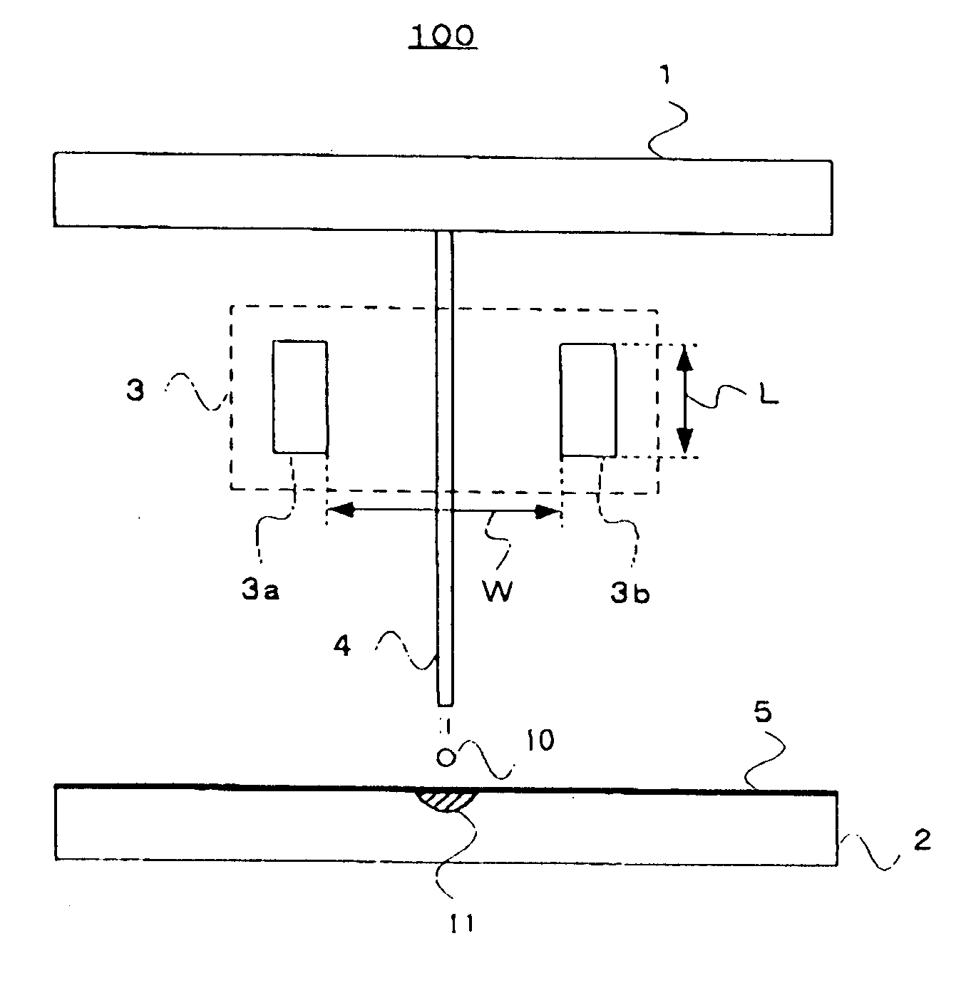
[0022] First, the electron emission element according to a first embodiment of the present invention will be explained with reference to FIG. 1 to FIG. 3. FIG. 1 schematically shows a configuration of an electron emission element 100 according to the first embodiment.

[0023] As shown in FIG 1, the electron emission element 100 includes a cathode substrate 1, an electron draw-out electrode 2, deflection electrode unit 3, an electron source (electron emission unit) 4 and an electron irradiation surface 5.

[0024] The cathode substrate 1 is made of material such as silicon. A voltage is applied to the cathode substrate 1 by a power supply (not shown), and the cathode substrate 1 functions as the cathode (cold cathode) in the electron emission element 100. On the cathode substrate 1, the electron source 4 is formed.

[0025] The electron source 4 functions as the thread-type electron emission unit, and a carbon nano-tube is used as the electron source 4 for example. The c...

second embodiment

[Second Embodiment]

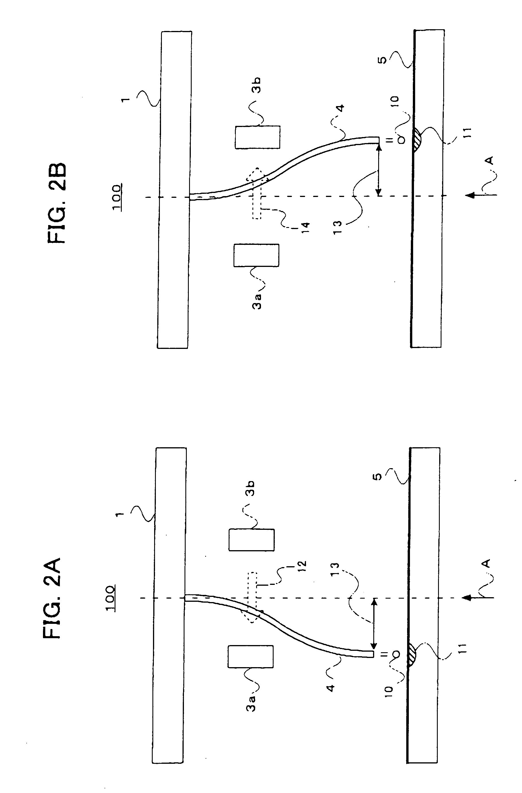
[0035] Next, the description will be given of an electron emission element 101 according to a second embodiment of the present invention with reference to FIGS. 4A and 4B.

[0036] As shown in FIG. 4A, the electron emission element 101 also includes the cathode substrate 1, the electron draw-out electrode 2, the deflection electrode unit 3, the electron source 4, and the electron irradiation surface 5, similarly to the first embodiment. Since the materials and the functions of them in the electron emission element are similar to those shown in the first embodiment, an explanation thereof is omitted.

[0037]FIG. 4B is a diagram showing the electron emission element 101 observed in a direction of an arrow B of FIG. 4A. As shown in FIG. 4B, the electron emission element 101 according to the second embodiment also includes the deflection electrode unit 3 including the pair of deflection electrodes 3a and 3b and the pair of deflection electrodes 3c and 3d around the elect...

third embodiment

[Third Embodiment]

[0040] Next, the description will be given of an electron emission element 102 according to a third embodiment of the present invention with reference to FIG. 5.

[0041] As shown in FIGS. 5A to 5C, the electron emission element 102 includes the cathode substrate 1, the electron draw-out electrode 2, the deflection electrode unit 3, a deflection electrode unit 6, the electron source 4 and the electron irradiation surface 5. The electron emission element 102 according to the third embodiment is different from the above-mentioned electron emission elements 100 and 101 in the first and second embodiments in that the deflection electrodes are provided at two positions in the longitudinal direction of the electron source 4. Since other components of the electron emission element 102 are similar to the above-mentioned components in the first and the second embodiments, an explanation thereof is omitted.

[0042] The deflection electrode units 3 and 6 according to the third e...


PUM


Abstract

By making a cathode substrate function as a cathode and applying a voltage to the cathode and an anode, an electron emission element emits an electron from an electron source provided on the cathode substrate, and irradiates the electron onto an electron irradiation surface formed on the anode surface. The electron source is thread-type and provided on the cathode substrate. A deflecting voltage generates the electric field around the electron source. The electron source including a charge receives a power from the generated electric field to curve. Therefore, an irradiation position of the electron moves on the electron irradiation surface. Since it becomes unnecessary to move the electron irradiation surface and the electron source, a configuration of the electron emission element or an apparatus including the electron emission element is not complicated, and can be miniaturized and simple. Further, since the electron source curves, a tip of the electron source and the electron irradiation surface can be close, and a size of a beam spot at the irradiation position can be maintained constant. Therefore, since a mechanism for correcting the size of the beam spot is unnecessary, the configuration of the electron emission element or the apparatus including the electron emission element can be much simpler.

Description

BACKGROUND OF THE INVENTION [0001] 1. Field of the Invention [0002] The present invention relates to an electron emission element irradiating an electron on a predetermined irradiation surface. [0003] 2. Description of Related Art [0004] There is known a technique of applying an electron emission element to a recording and reproduction apparatus and an image display apparatus. Particularly, there is known a following technique of moving a position on an electron irradiation surface (hereinafter referred to as “irradiation posistion”) at which an electron from an electron source included in the electron emission element is irradiated. [0005] For example, there is proposed a technique of changing a recording position on a recording medium by moving the recording medium in a recording apparatus performing recording and reproduction by using an electron beam. This method is disclosed in Japanese Patent Application Laid-open under No. 9-7240. There is also proposed a technique of making ...

Claims


Application Information

Patent Timeline
Patent Type & Authority Applications(United States)
IPC IPC(8): H01J29/08H01J1/304H01J3/02H01J63/04
CPCH01J3/021
Inventor OKANO, MAKOTOIMAI, TETSUYAKUMASAKA, OSAMU
Owner PIONEER CORP
Why Eureka
Try Eureka