Memory interface control circuit and memory interface control method

a control circuit and memory technology, applied in the field of memory interface control circuit and memory interface control method for reading data from a memory, can solve the problems of difficult to determine the timing at which the receiver accepts data, and the placement of a plurality of rams is still restricted, and achieves high glitch noise resistance

Active Publication Date: 2005-09-29
NEC CORP
View PDF6 Cites 39 Cited by
  • Summary
  • Abstract
  • Description
  • Claims
  • Application Information

AI Technical Summary

Benefits of technology

[0022] It is an object of the present invention to provide a memory interface control circuit and memory interface control method capable of relaxing a RAM placement restriction and ensuring a high glitch noise resistance.

Problems solved by technology

If the wiring lengths from the memory (DDR SDRM) to a controller are different, time required until data reaches to a receiver (flight time) is also different, thereby, it is difficult to determine a timing at which the receiver accepts data.
Even if the mask is set at a specific timing to prevent the glitch noise from being superimposed on the DQS, the placement of a plurality of RAMs are still restricted.

Method used


Image

  • Memory interface control circuit and memory interface control method
  • Memory interface control circuit and memory interface control method
  • Memory interface control circuit and memory interface control method

Examples


Embodiment Construction

[0046] A preferred embodiment of the present invention will be described hereinafter in detail with reference to the accompanying drawings.

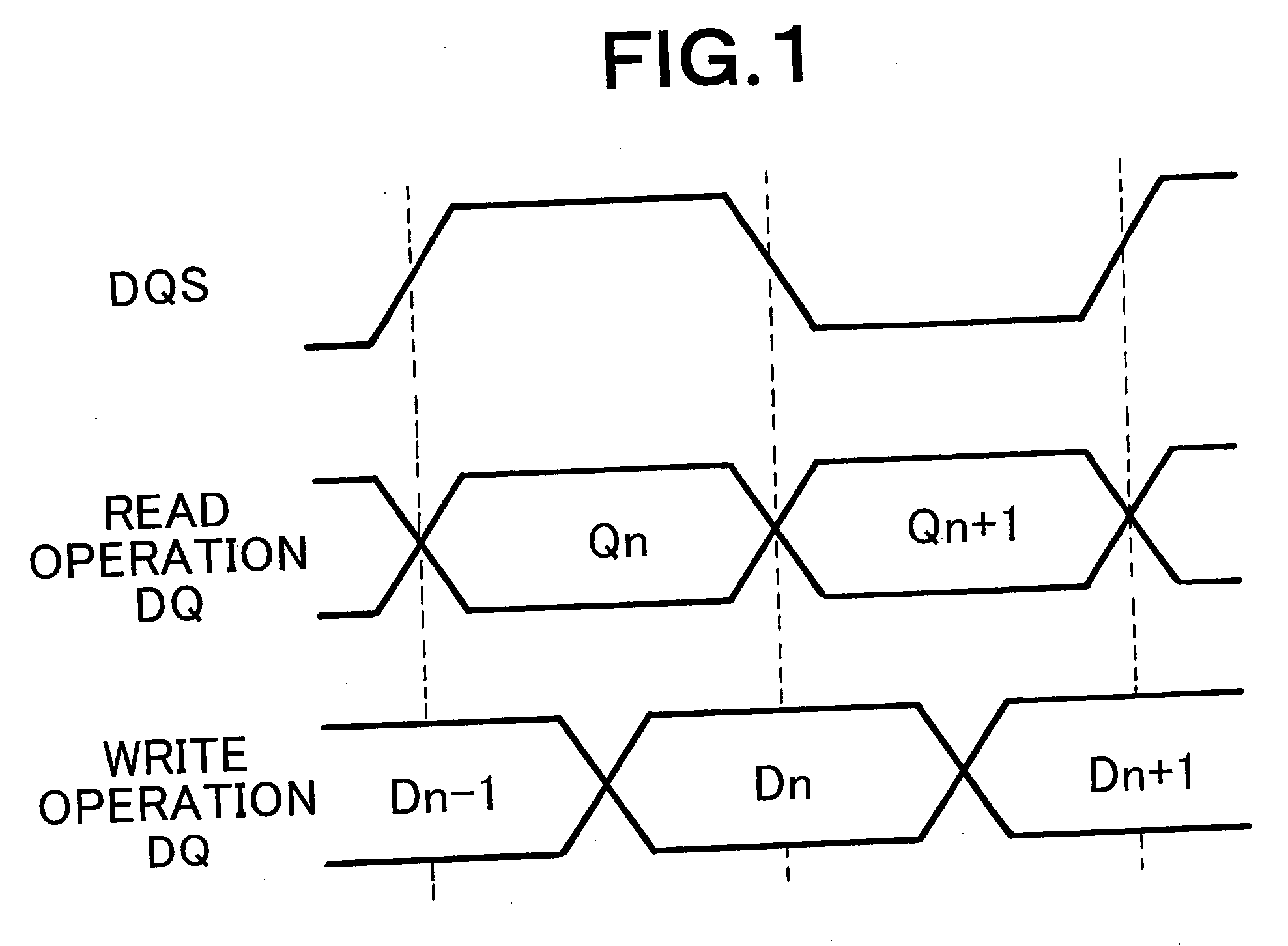
[0047] The present invention is characterized in that a glitch noise resistance of a data strobe signal (DQS) can be improved in data transfer between a memory (particularly a DDR2-SDRAM) and a LSI, and in that a physical placement restriction relative to the LSI with which the memory performs the data transfer.

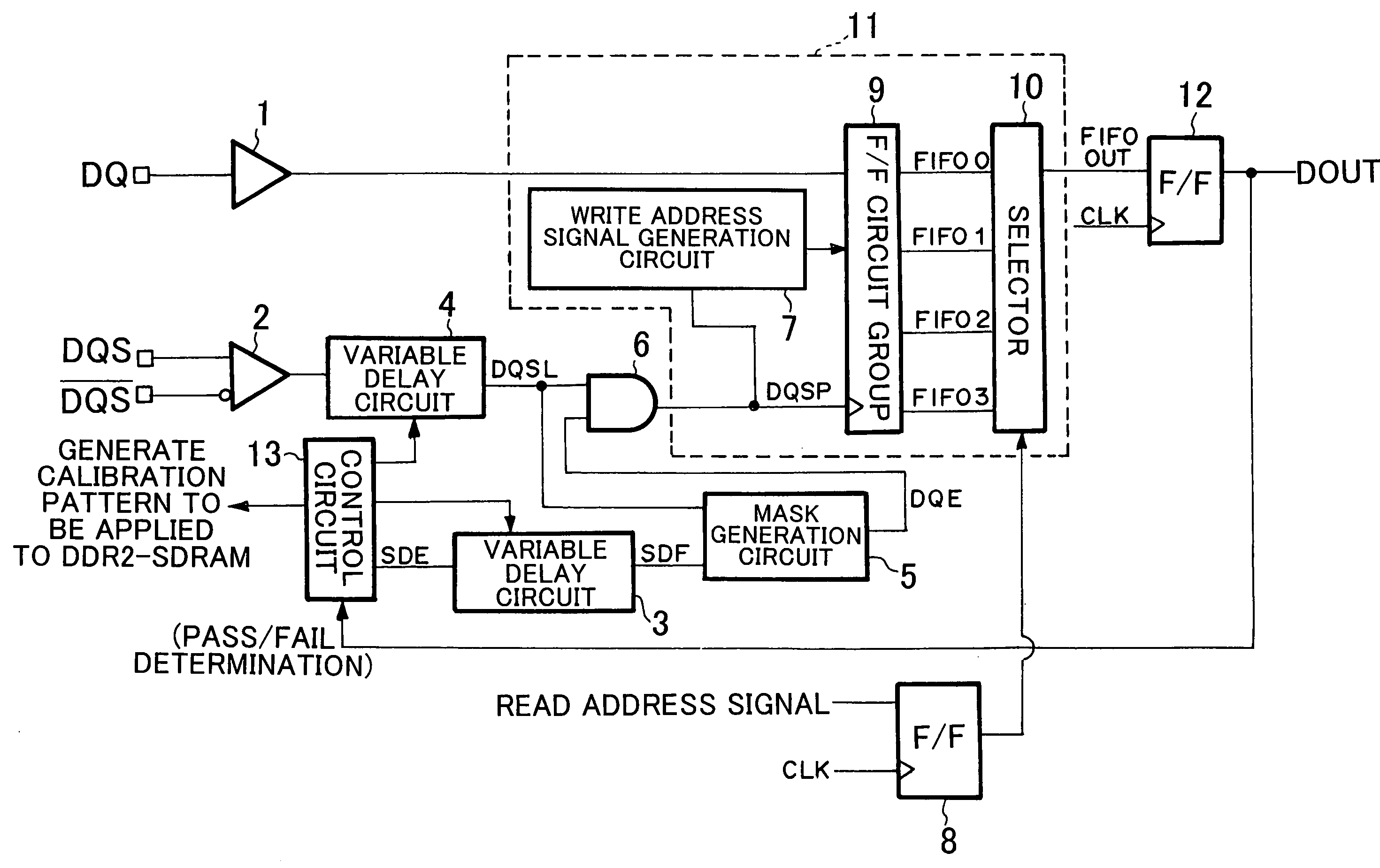
[0048]FIG. 6 is a block diagram that depicts a configuration of a memory interface control circuit according to the embodiment of the present invention. In FIG. 6, an I / O buffer 1 is an input buffer that receives data read from the DDR2-SDRAM. An I / O buffer 2 is an input buffer that receives a data strobe signal DQS read from the SDR2-SDRAM. The data strobe signal DQS is a balance input / output in the SDR2-SDRAM. Although the I / O buffers 1 and 2 are originally bidirectional buffers, they are illustrates as input buffers since this embodim...


PUM


Abstract

According to one embodiment, one variable delay circuit adjusts a data strobe signal to be delayed, a control circuit generates an auxiliary signal, another variable delay circuit adjusts the auxiliary signal to be delayed, a mask generation circuit generates a mask signal based on the delayed data strobe signal and the delayed auxiliary signal, and an AND circuit applies the mask signal to the delayed data strobe signal, thereby generating a data strobe signal without a glitch. A write address signal generation circuit generates a control signal for controlling a flip-flop group based on the data strobe signal without the glitch, and the flip-flop group stores read data according to the control signal. A selector selects data from among pieces of data stored in the flip-flop group according to the read address signal.

Description

BACKGROUND OF THE INVENTION [0001] 1. Field of the Invention [0002] The present invention relates to a memory interface control circuit and memory interface control method for reading data from a memory. More specifically, the present invention relates to a memory interface control circuit and memory interface control method for reading data from a double data rate 2-synchronous random access memory (hereinafter, “DDR2-SDRAM”). [0003] 2. Description of the Related Art [0004] DDR-SDRAM has experienced substantial growth over the past several years. The DDR-SDRAM is a synchronous dynamic random access memory (“synchronous DRAM” or “SDRAM”) having a high-rate data transfer function called “double data rate (“DDR”) mode”. In the DDR mode, data can be read and written at both rising and falling of a clock signal which is provided for synchronizing respective circuits in a computer. [0005] The DDR-SDRM inputs and outputs data at a frequency twice as high as that of an external clock, so t...

Claims


Application Information

Patent Timeline
Patent Type & Authority Applications(United States)
IPC IPC(8): G11C7/10G11C7/22G11C11/407
CPCG11C7/1051G11C2207/2254G11C7/1066G11C7/106A47G19/2227A47G19/2272A47G2200/106A47G2019/2294
Inventor AOKI, MUTSUMI
Owner NEC CORP
Why Eureka
Try Eureka