Nitride semiconductor light emitting device and method of manufacturing the same

Active Publication Date: 2005-10-06
SAMSUNG ELECTRONICS CO LTD
View PDF23 Cites 85 Cited by
  • Summary
  • Abstract
  • Description
  • Claims
  • Application Information

AI Technical Summary

Benefits of technology

[0012] Therefore, the present invention has been made in view of the above problems, and it is an object of the present invention to provide a nitride semiconductor light emitting device having patterns formed on the upper and lower surfaces of a substrate from

Problems solved by technology

The above-mentioned light emitting devices, especially the GaN-based white light emitting device, have low light emitting efficiency, which is the greatest problem with the light emitting devices.
The conventional GaN-based white light emitting device has a problem in that the efficiency at which light is emitted from the light emitting device is very low.
The major obstacle to emission of light from the light emitting device is internal total reflection.
Furthermore, the remain

Method used


Image

  • Nitride semiconductor light emitting device and method of manufacturing the same
  • Nitride semiconductor light emitting device and method of manufacturing the same
  • Nitride semiconductor light emitting device and method of manufacturing the same

Examples


Embodiment Construction

[0031] Now, preferred embodiments of the present invention will be described in detail with reference to the accompanying drawings.

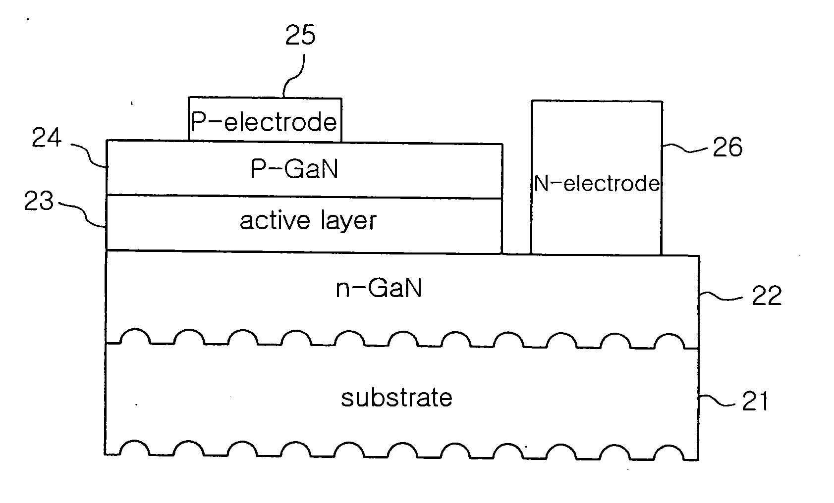
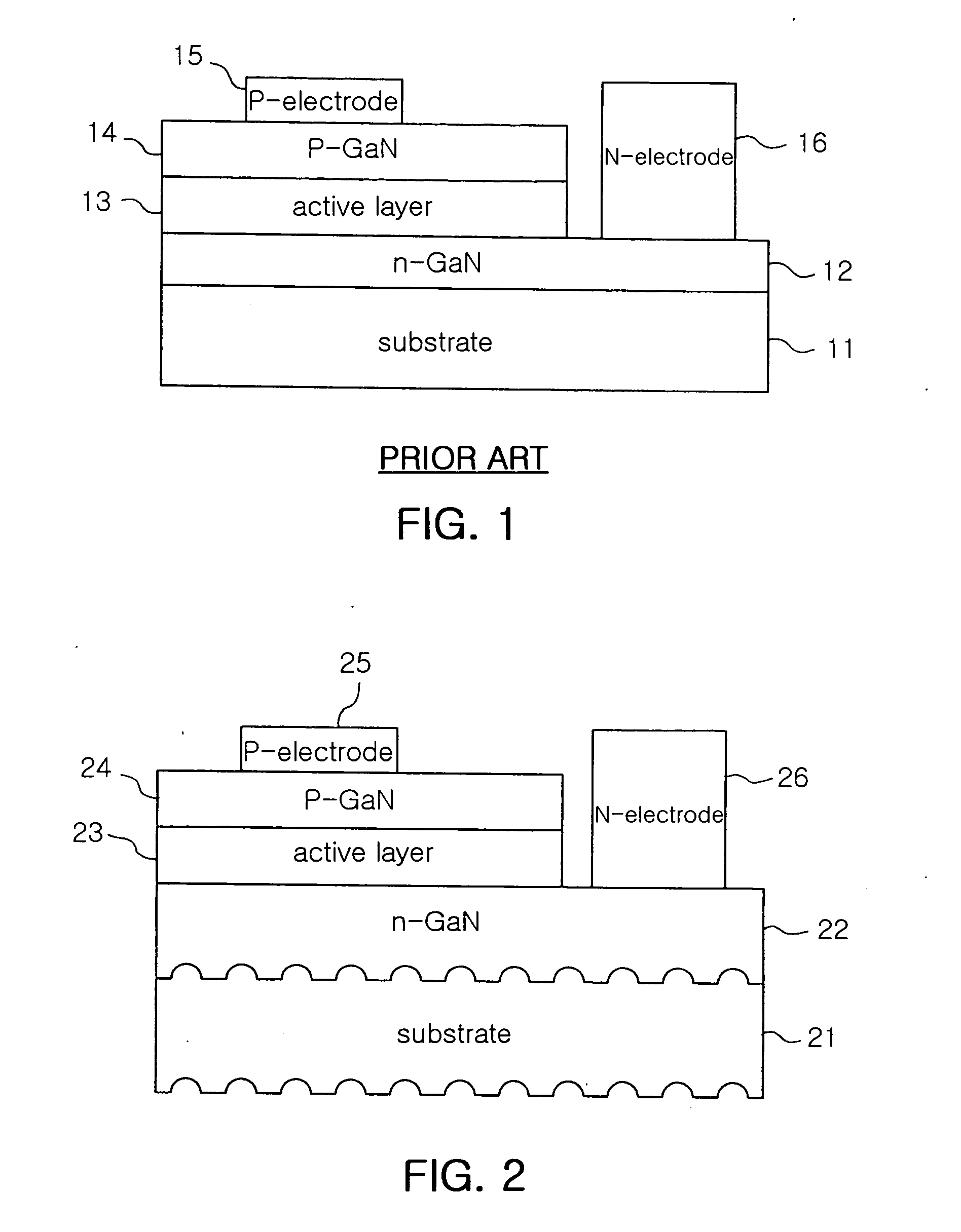
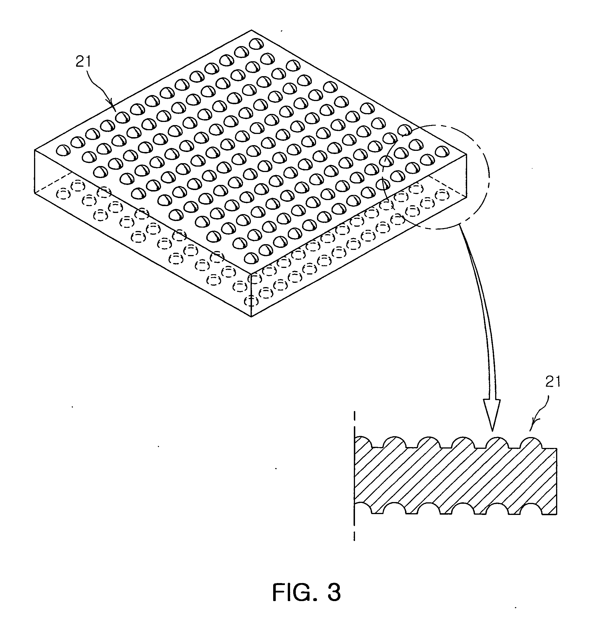
[0032]FIG. 2 is a side view, in section, showing the basic structure of a nitride semiconductor light emitting device according to the present invention. The nitride semiconductor light emitting device comprises: a substrate 21 having upper and lower surfaces on which predetermined concave and convex patterns are formed such that light can be incident within a critical angle, the substrate 21 allowing a gallium nitride-based semiconductor material to be grown thereon; an n-type nitride semiconductor layer 22 formed on the upper surface of the substrate 21; an active layer 23 formed on the upper surface of the n-type nitride semiconductor layer 22 such that the n-type nitride semiconductor layer 22 is partially exposed; a p-type nitride semiconductor layer 24 formed on the upper surface of the active layer 23; a p-electrode (P-electrode) 25 formed on the...


PUM


Abstract

Disclosed herein is a nitride semiconductor light emitting device having patterns formed on the upper and lower surfaces of a substrate from which light is emitted in a flip chip bonding structure wherein the patterns are capable of changing light inclination at the upper and lower surfaces of the substrate to decrease total reflection at the interfaces, thereby improving light emitting efficiency. The nitride semiconductor light emitting device comprises a substrate having upper and lower surfaces on which predetermined patterns are formed such that light can be incident within a critical angle, the substrate allowing a gallium nitride-based semiconductor material to be grown thereon, an n-type nitride semiconductor layer formed on the upper surface of the substrate, an active layer formed on the upper surface of the n-type nitride semiconductor layer such that the n-type nitride semiconductor layer is partially exposed, a p-type nitride semiconductor layer formed on the upper surface of the active layer, a p-electrode formed on the upper surface of the p-type nitride semiconductor layer, and an n-side electrode formed on the partially exposed n-type nitride semiconductor layer.

Description

RELATED INVENTION [0001] The present application is based on, and claims priority from, Korean Application Number 2004-21801, filed Mar. 30, 2004, the disclosure of which is incorporated by reference herein in its entirety. BACKGROUND OF THE INVENTION [0002] 1. Field of the Invention [0003] The present invention relates to a nitride semiconductor light emitting device, and more particularly to a nitride semiconductor light emitting device having patterns formed on the upper and lower surfaces of a substrate wherein the patterns are capable of changing light inclination at the upper and lower surfaces of the substrate to decrease total reflection, thereby improving light emitting efficiency. Also, the present invention relates to a method of manufacturing the same. [0004] 2. Description of the Related Art [0005] Lately, a nitride semiconductor, such as GaN, has been widely used as a photoelectric material or an essential material for electronic devices by virtue of its excellent phys...

Claims


Application Information

Patent Timeline
IPC IPC(8): H01L21/00H01L29/22H01L33/22H01L33/32H01L33/38H01L33/62
CPCH01L33/007H01L33/22H01L33/32Y10S257/918
Inventor LEE, JAE HOONLEE, JEONG WOOKKIM, HYUN KYUNGKIM, YONG CHUN
Owner SAMSUNG ELECTRONICS CO LTD
Why Eureka
Try Eureka