In-line wafer surface mapping

a surface mapping and wafer technology, applied in semiconductor/solid-state device testing/measurement, lapping machines, instruments, etc., can solve problems such as device characteristics that fail and/or vary unacceptably across the substrate, and pattern distortion and/or misalignment may occur at various locations, so as to increase the likelihood that substrate surface non-uniformities will result in device feature defects

Inactive Publication Date: 2005-10-13
TAIWAN SEMICON MFG CO LTD
View PDF3 Cites 16 Cited by
  • Summary
  • Abstract
  • Description
  • Claims
  • Application Information

AI Technical Summary

Benefits of technology

[0004] It is therefore important for the substrate surface to be uniformly level and likewise important to be able to monitor the topographical uniformity of the substrate surface. This is especially true as device feature sizes shrink into the nanometer regime while substrate sizes increase to 12 inch diameters or greater, increasing the likelihood that substrate surface non-uniformities will result in device feature defects. It would be especially useful to be able to obtain such topographical data on the raw substrate, during the in-line processing of the substrate and responsive to the detection of

Problems solved by technology

If the substrate surface is not at the expected location, pattern distortion and/or misalignment may result.
If the substrate surface is not uniformly level, then such pattern distortion and/or misalignment may occur at various locations across the substrate.
This may result in device characteristics that fail and/or vary unacceptably across the substrate.
This is especially true as device feature sizes shrink into the nanometer regime whil

Method used


Image

  • In-line wafer surface mapping
  • In-line wafer surface mapping
  • In-line wafer surface mapping

Examples


Embodiment Construction

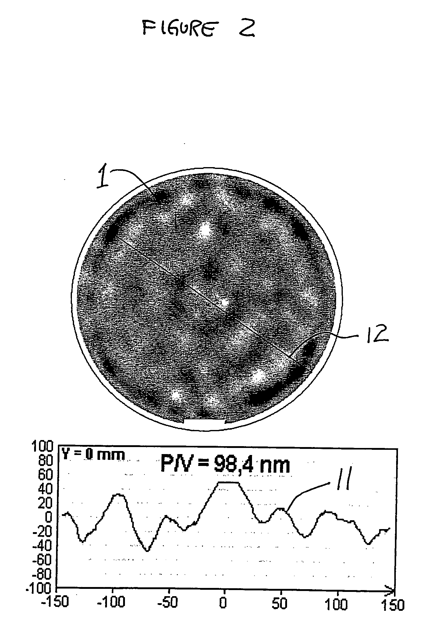
[0020]FIG. 2 is a plan view that illustrates an uneven substrate surface of an exemplary substrate. Alternatively stated, the substrate surface has a non-uniform topography. The topography of the uneven surface is represented by plot 11 which is taken along arbitrary direction 12 in the exemplary embodiment. The higher and lower sections in plot 11 correspond to raised and depressed sections of substrate 1, respectively, and are exemplary only. Such information is conventionally gathered when substrate 1 is in raw form and prior to any of the processing operations have been performed upon the substrate 1. A number of plots 11 may be taken at various locations and in various directions along the surface of substrate 1 to provide for the topographical mapping of the substrate.

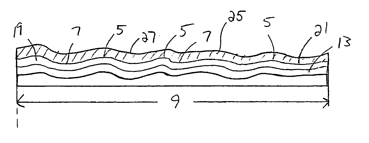
[0021]FIG. 3 is a cross-sectional view of exemplary substrate 1. Substrate 1 may be any of various substrates such as an N- or P-type silicon substrate, a gallium arsenide substrate, a sapphire substrate or othe...


PUM

PropertyMeasurementUnit
Diameteraaaaaaaaaa
Diameteraaaaaaaaaa
Dielectric polarization enthalpyaaaaaaaaaa

Abstract

A method and apparatus for the topographical profiling of a raw substrate is carried out during in-line processing of the substrate during which additional films and structures have been formed over the raw substrate surface. The method includes forming a dielectric film over the substrate surface and forming a metal film over the dielectric film. The structure is polished and monitored during various stages of the polishing operation. An interferometer is used to monitor the surface being polished and to distinguish between regions where metal remains and regions in which metal has been removed and the underlying dielectric material exposed. Topographical data, such as a substrate map, is generated by monitoring the time at which the metal film is removed from various spatial locations across the substrate. The substrate map may be generated during polishing, for in-line monitoring.

Description

FIELD OF THE INVENTION [0001] The present invention relates, most generally, to semiconductor devices and methods for forming the same. More particularly, the present invention relates to a method and apparatus for mapping raw substrate topography during in-line processing. BACKGROUND [0002] Semiconductor devices such as integrated circuits and the like, are formed by performing a series of processing operations upon a substrate to form accurately sized and precisely aligned device features. The device features are formed from various conductive and dielectric films that are formed on the substrate. The processing operations include multiple photolithographic patterning processes used to pattern the various conductive and dielectric films and also to define regions in the films or the substrate into which various impurities will be introduced. It is critical to accurately define the various device features so that they are accurately sized, positioned and aligned to tight tolerances...

Claims


Application Information

Patent Timeline
IPC IPC(8): B24B1/00B24B37/04B24B49/12
CPCB24B49/12B24B37/005
Inventor YANG, WAN-CHENG
Owner TAIWAN SEMICON MFG CO LTD
Why Eureka
Try Eureka