
Light-emitting device

a technology of light-emitting devices and elements, which is applied in the direction of static indicating devices, electroluminescent light sources, instruments, etc., can solve the problems of affecting the electrical current and undergoing a change, the change of drain current i/sub>ds/sub>is very susceptible to a change in the gate-source voltage, and the effect of reducing the rate of deterioration of the el elemen

Inactive Publication Date: 2005-10-20
SEMICON ENERGY LAB CO LTD
View PDF39 Cites 36 Cited by
  • Summary
  • Abstract
  • Description
  • Claims
  • Application Information

AI Technical Summary

Benefits of technology

This approach results in a high aperture ratio with reduced current density and less deterioration of the EL element, maintaining brightness and image quality despite increased TFT size, and minimizes the effect of shrinkage on the light-emitting area.

Problems solved by technology

However, if the resistance of the EL element 1506 varies due to a change in the temperature or aging, the electric current is affected thereby and undergoes a change.
Further, the electric current is seriously affected by a change in the gate-source voltage VGS during the holding period.
Therefore, a change in the drain current IDS is very susceptible to a change in the gate-source voltage |VGS|.

Method used


Image

  • Light-emitting device
  • Light-emitting device
  • Light-emitting device

Examples


embodiment 1

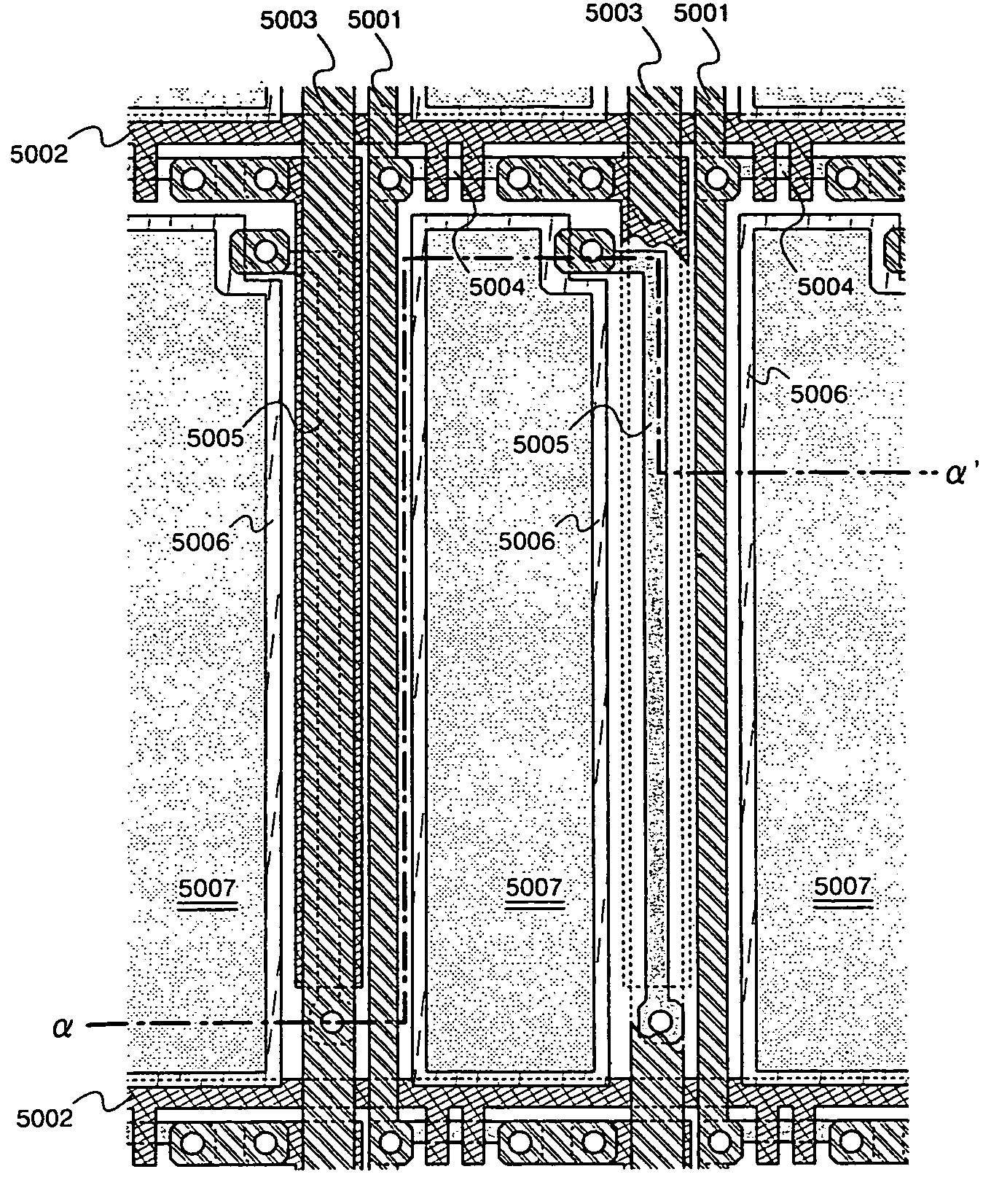
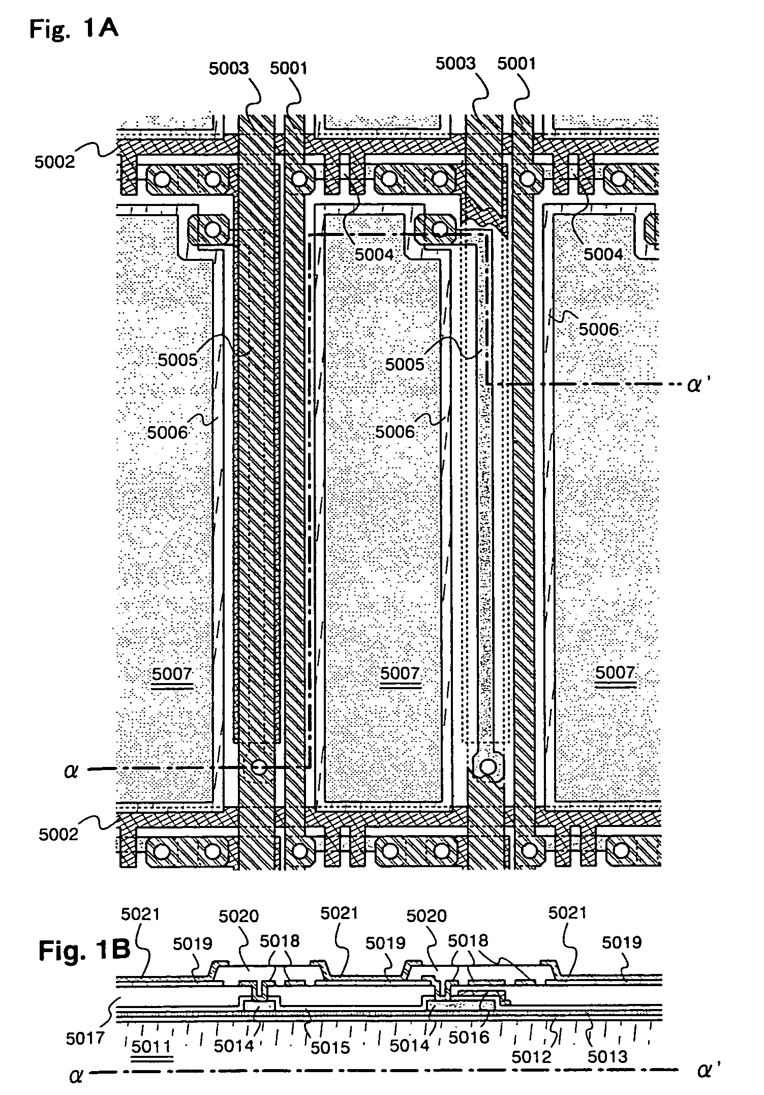
[0076] First, the embodiment will be described with reference to FIG. 1. Here, the light-emitting device produces a full-color display and wherein either the source regions or the drain regions of the driving TFTs of pixels R for emitting light of red color are connected to a current supply line for red color, either the source regions or the drain regions of the driving TFTs of pixels G for emitting light of green color are connected to a current supply line for green color, and either the source regions or the drain regions of the driving TFTs of pixels B for emitting light of blue color are connected to a current feed line for blue color. The EL materials of the EL elements of R, G and B are separately applied like stripes.

[0077] In FIG. 1, the partitioning walls are covering the regions other than the light-emitting areas 5007. Among the partitioning walls 5020, those partitioning walls formed in parallel with the stripes serve as coloring margins. The places where there exist ...

embodiment 2

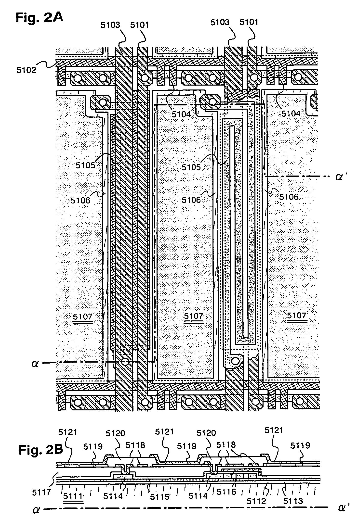
[0080] When three transistors are used for constituting a pixel, the two transistors, namely, a switching TFT and an erasing TFT, excluding the driving TFT, are linearly arranged to maintain aperture ratio in order to realize a further simplified opening portion. The opening portion of a simple shape which is close to a rectangular shape helps decrease the effect of shrink.

embodiment 3

[0081] In determining the channel length and the channel width of the driving TFT, it is necessary to increase the channel length and the channel width as much as possible and, when the driving TFT is to be operated in the saturated region, to select the channel length to be larger than the channel width, so that the gate-source voltage VGS is little affected by the threshold voltage. Upon increasing the channel length, the characteristics of the driving TFT are more flattened in the saturated region. Here, if the gate-source voltage VGS is increased too much, problems concerning the consumption of electric power and breakdown voltage of the driving TFTs will arise. It is therefore desired that the channel length and the channel width are so adjusted that |VGS| is not lower than 4 V but is not higher than 14 V.

[0082] According to the embodiments 1 to 3, the size of the driving TFT is increased and the channel length L is increased relative to the channel width W, making it possible...


PUM


Abstract

A light-emitting device which realizes a high aperture ratio and in which the quality of image is little affected by the variation in the characteristics of TFTs. A large holding capacitor Cs is not provided in the pixel portion but, instead, the channel length and the channel width of the driving TFTs are increased, and the channel capacitance is utilized as Cs. The channel length is selected to be very larger than the channel width to improve current characteristics in the saturated region, and a high VGS is applied to the driving TFTs to obtain a desired drain current. Therefore, the drain currents of the driving TFTs are little affected by the variation in the threshold voltage. In laying out the pixels, further, wiring is arranged under the partitioning wall and the driving TFTs are arranged under the wiring in order to avoid a decrease in the aperture ratio despite of an increase in the size of the driving TFT. In the case of the 3-transistor pixels, the switching TFT and the erasing TFT are linearly arranged to further increase the aperture ratio.

Description

BACKGROUND OF THE INVENTION [0001] 1. Field of the Invention [0002] This invention relates to an electroluminescence (EL) element, and to a method of driving an electronic display manufactured by forming thin-film transistors (hereinafter abbreviated as TFTs) on a substrate. Particularly, the invention relates to a light-emitting device which uses semiconductor elements (elements formed from a semiconductor thin film). The invention further relates to electronic devices using the light-emitting device as a display unit. [0003] In this specification, the EL elements include the ones which utilize emission of light from singlet excitons (fluorescence) and the ones which utilize the emission of light from triplet excitons (phosphorescence). [0004] 2. Description of the Related Art [0005] In recent years, light-emitting devices having EL elements have been vigorously developed as self light emitting elements. Unlike the liquid crystal display devices, the light-emitting device is self l...

Claims


Application Information

Patent Timeline
Patent Type & Authority Applications(United States)
IPC IPC(8): G09G3/32H01L27/32H05B44/00
CPCG09G3/3233G09G2300/0426G09G2300/0842G09G2310/0254G09G2320/043H01L27/3211H01L27/3262H01L2924/0002H01L27/3265H01L27/3295H01L33/08H01L2924/00H01L27/1255H10K59/35H10K59/122H10K59/1213H10K59/1216G09G3/30
Inventor OSAME, MITSUAKIANZAI, AYAKOYAMA, JUNUDAGAWA, MAKOTOHAYAKAWA, MASAHIKOYAMAZAKI, SHUNPEI
Owner SEMICON ENERGY LAB CO LTD
Learn More