Apparatus and method for secondary electron emission microscope

a secondary electron emission microscope and electron emission technology, applied in the direction of heat measurement, semiconductor/solid-state device testing/measurement, instruments, etc., can solve the problems of optical beams sensitive, whole chips may fail, and it is difficult to establish electrical connections, etc., to achieve low current density and high signal-to-noise ratio

Inactive Publication Date: 2006-01-10
KLA TENCOR TECH CORP
View PDF14 Cites 0 Cited by
  • Summary
  • Abstract
  • Description
  • Claims
  • Application Information

AI Technical Summary

Benefits of technology

[0019]The comparative speed advantage in SEEM, i.e. the maximum pixel rate, is limited mainly by the ‘dwell time’ and the ‘current density.’ The minimum dwell time that a beam must spend looking at a given image is determined by the acceptable Signal-to-Noise ratio of the image. The maximum current density is determined by such practical considerations as available gun brightness and possible sample damage. Because the focused beam of primary electrons in SEM must scan the beam across the entire surface to be inspected, the maximum practical pixel rate in Scanning Electron Microscopy is less than or equal to 100 million pixels / second (100 MHz). In Secondary Electron Emission. Microscopy (SEEM), a large two-dimensional area of the sample is imaged in parallel without the need for scanning. The maximum pixel rate in SEEM is greater than 800 million pixels / second (800 MHz). The dwell time of the beam in SEEM may correspondingly be much longer than in SEM, and this permits a much lower current density while still maintaining a high Signal-to-Noise ratio. Thus, SEEM has the capability of investigating more sensitive sample surface structures while requiring lower brightness electron beam sources.

Problems solved by technology

If one of these holes or vias becomes clogged, it will be impossible to establish this electrical connection and the whole chip may fail.
Optical beams are sensitive to problems of color noise and grain structures whereas electron beams are not.
Oxide trenches and polysilicon lines are especially prone to false positives with optical beams due to grain structure.
However, raster scanning a surface with scanning electron microscopy is slow because each pixel on the surface is collected sequentially.
Moreover, a complex and expensive electron beam steering system is needed to control the beam pattern.
This charge build-up problem limits the utility of PEEM for imaging insulators.
However, LEEM suffers from a similar charge build-up problem since electrons are directed at the sample surface, but not all of the electrons are energetic enough to leave the surface.
In LEEM, negatively-charged electrons accumulate on the surface, which repels further electrons from striking the sample, resulting in distortions and shadowing of the surface.
Several prior art publications have discussed a variety of approaches using electron beams in microscopy, but none have determined how to do so with parallel imaging at the same time the charge build-up problem is eliminated.
Veneklasen notes generally that the LEEM electron potential difference between the source and sample can be adjusted between zero and a few keV, but he does not recognize the charging problem or propose a solution to it.

Method used


Image

  • Apparatus and method for secondary electron emission microscope
  • Apparatus and method for secondary electron emission microscope
  • Apparatus and method for secondary electron emission microscope

Examples


Embodiment Construction

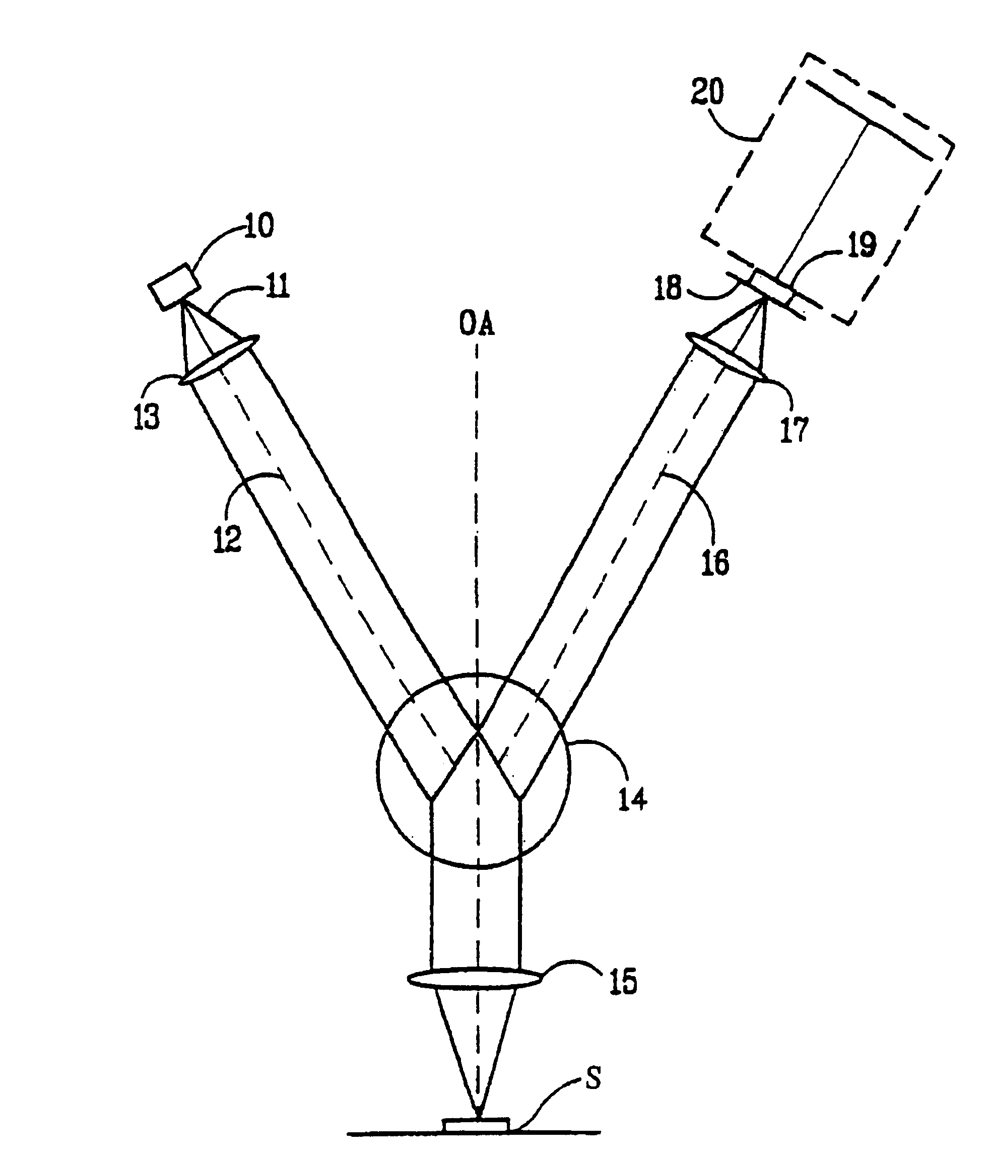
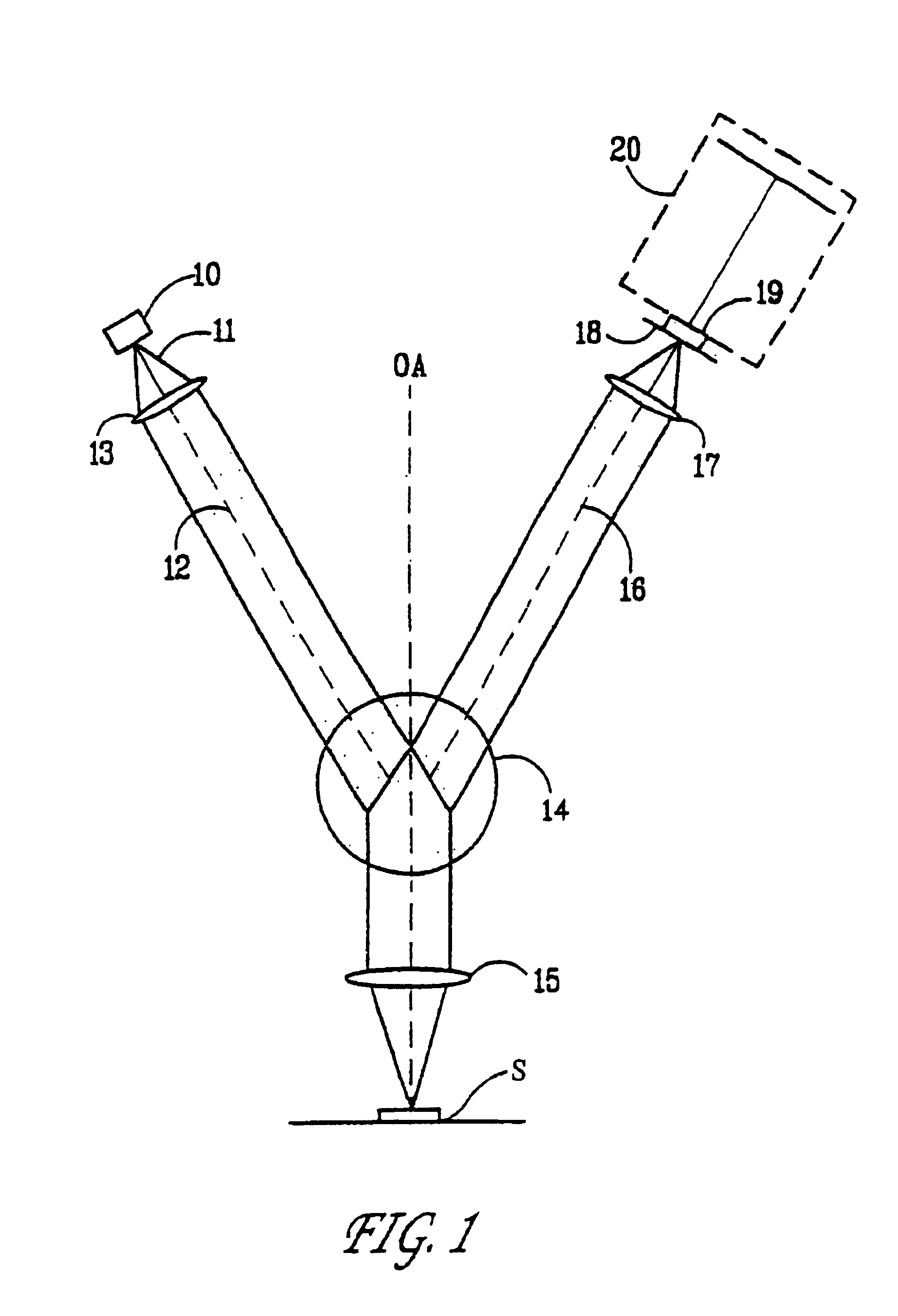
[0028]FIG. 1 shows the basic configuration for the Secondary Electron Emission Microscopy (SEEM) apparatus of the present invention. An electron gun source 10 emits a beam 11 of primary electrons e1 along path 12. The electron beam 11 is collimated by electron lens 13 and continues along path 12. Magnetic beam separator 14 then bends the collimated electron beam 11 to be incident along electron optical axis OA normal to the surface to be inspected. Objective electron lens 15 focuses the primary electrons, e1, into a beam having a spot size in the range 1-10 mm and an incident energy on the order of 1 keV on sample S.

[0029]Primary electrons e1 incident on the sample S produce secondary electrons e2 which travel back along the axis OA perpendicular to the inspection surface to objective electron lens 15, where they are recollimated. Magnetic beam separator 14 bends the electrons to travel along image path 16. The electron beam along image path 16 is focused by projection electron lens...


PUM

PropertyMeasurementUnit
widthaaaaaaaaaa
widthaaaaaaaaaa
sizeaaaaaaaaaa

Abstract

An apparatus and method for inspecting a surface of a sample, particularly but not limited to a semiconductor device, using an electron beam is presented. The technique is called Secondary Electron Emission Microscopy (SEEM), and has significant advantages over both Scanning Electron Microscopy (SEM) and Low Energy Electron Microscopy (LEEM) techniques. In particular, the SEEM technique utilizes a beam of relatively high-energy primary electrons having a beam width appropriate for parallel, multi-pixel imaging. The electron energy is near a charge-stable condition to achieve faster imaging than was previously attainable with SEM, and charge neutrality unattainable with LEEM. The emitted electrons may be detected using a time delay integration detector.

Description

CROSS-REFERENCE TO RELATED APPLICATIONS[0001]This is a continuation application of and claims priority in U.S. patent application Ser. No. 10 / 033,452 entitled APPARATUS AND METHOD FOR SECONDARY ELECTRON EMISSION MICROSCOPE, filed Nov. 2, 2001 now U.S. Pat. No. 6,713,759 which is a continuation of U.S. patent application Ser. No. 09 / 613,985 entitled APPARATUS AND METHOD FOR SECONDARY ELECTRON EMISSION MICROSCOPE, filed Jul. 11, 2000 now abandoned which is a continuation of U.S. patent application Ser. No. 09 / 354,948, entitled APPARATUS AND METHOD FOR SECONDARY ELECTRON EMISSION MICROSCOPE, filed Jul. 16, 1999, which was issued as U.S. Pat. No. 6,087,659 on Jul. 11, 2000, and which is a divisional application of U.S. patent application Ser. No. 08 / 964,544,entitled APPARATUS AND METHOD FOR SECONDARY ELECTRON EMISSION MICROSCOPE, filed Nov. 5, 1997 now U.S. Pat. No. 5,973,323.BACKGROUND OF THE INVENTION[0002]1. Technical Field[0003]The present invention relates generally to an apparatus...

Claims


Application Information

Patent Timeline
Patent Type & Authority Patents(United States)
IPC IPC(8): G01N23/00G21K7/00G01N23/225G01Q30/02H01J37/244H01J37/28H01J37/285H01L21/66
CPCH01J37/285
Inventor ADLER, DAVID L.WALKER, DAVID J.BABIAN, FREDWOLFE, TRAVIS
Owner KLA TENCOR TECH CORP
Why Eureka
Try Eureka