Time-mode analog computation circuits and methods

a computation circuit and time-mode technology, applied in the field of analog computational circuits, can solve the problems of limited dynamic range (dr), computational circuits that exhibit poor signal-to-noise ratio (snr), and/or high power consumption, and achieve the effect of overcompensating the limitations of voltage-based scaling

Inactive Publication Date: 2005-10-20
UNIV OF FLORIDA RES FOUNDATION INC
View PDF6 Cites 9 Cited by
  • Summary
  • Abstract
  • Description
  • Claims
  • Application Information

AI Technical Summary

Benefits of technology

[0006] The present invention provides the circuit building blocks and techniques for computations using analog temporal signal function representations for both inputs and outputs. The invention enables computations using the timing of asynchronous events, for example. The computations performed with the circuits and methods of the invention produce results that can be expressed as time. For example, the result of a computation with the invention can be a time-based parameter corresponding to the timing of a signal output. This obviates the need for translation of temporal signals to an analog or digital form. The invention further overcomes limitations to scaling inherent in voltage-based and current-based computation circuits.

Problems solved by technology

With technology scaling, the degrees of freedom for using voltages and currents for computations are generally more restricted.
This can result in computational circuits that exhibit a poor signal-to-noise ratio (SNR), very limited Dynamic Range (DR), and / or high power consumption.
These factors are likely to be significant impediments to the development of more efficient and more effective analog computation circuits in the future, especially in light of the problems posed by technology scaling.
Complementary metal-oxide semiconductor (CMOS) process technology, in particular, has lead to scaling that requires significant reductions in the chip “real estate” consumed by analog circuitry.
Moreover, as CMOS process technology continues to shrink the usable voltage swing in such circuits, traditional analog circuit designs have been rendered less practicable.

Method used


Image

  • Time-mode analog computation circuits and methods
  • Time-mode analog computation circuits and methods
  • Time-mode analog computation circuits and methods

Examples


examples

[0080] The present invention is further illustrated by the following specific examples, which should not be construed as limiting the scope or content of the invention in any way.

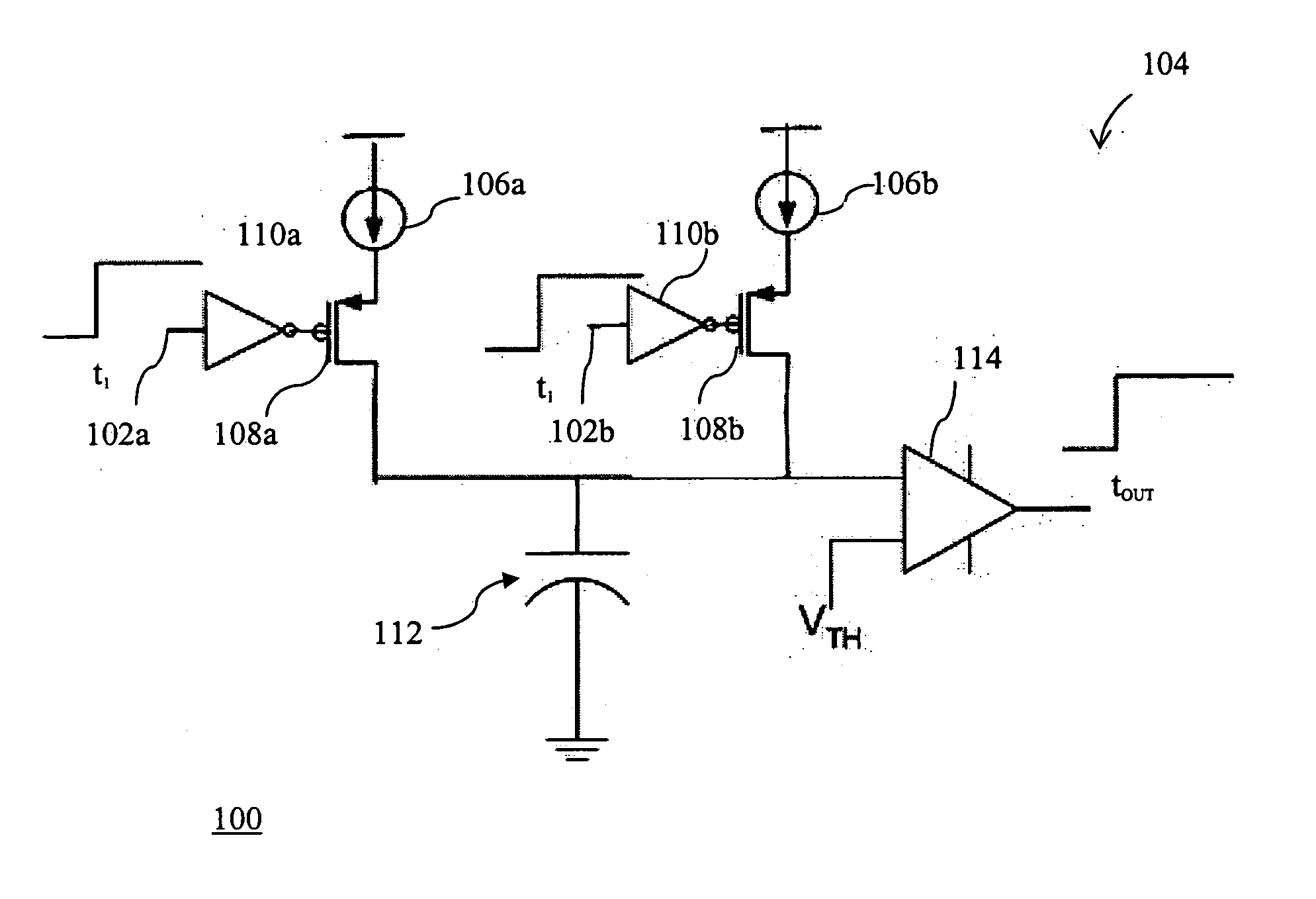
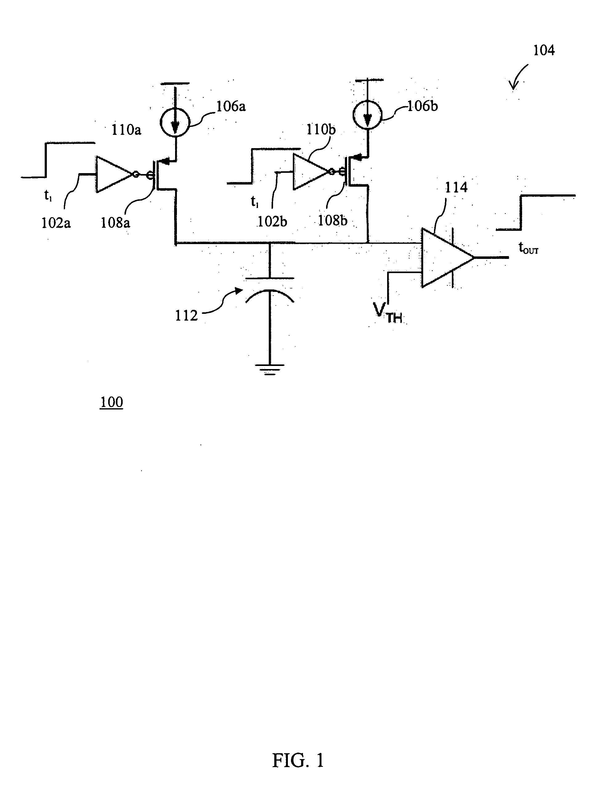
[0081] Circuit 100 shown in FIG. 1 was simulated and prototype time-mode circuits according to the invention measured under a variety of conditions. FIG. 8 shows Cadence-Spectre simulation results where circuit 100 was used to compute the arithmetic mean of two input steps, t1, and t2. The values of t1, t2, C, VTH and I(I1=I2) used in the simulation were 200 μs, 400 μs, 20 pF, 2.5V and 50 nA, respectively. The output expected from circuit 100 from equation (1) above is 800 μs which includes a 500 μs offset term (CVTH / I) thus computing the actual mean of t1 and t2 of 300 μs. The output obtained from simulations performed was 801 μs. It is noted that random variations in this delay and in the current sources can lead to inaccuracies in the calculations generated.

[0082]FIG. 9 shows measured data from a fabri...


PUM


Abstract

A time-mode analog computation circuit is provided. The time-mode analog computation circuit includes one or more inputs for receiving one or more temporal input signals. The time-mode analog computation circuit further includes circuitry for performing a mathematical operation based on the one or more temporal input signals. A result of the mathematical operation is expressed in a timing of an output signal generated by the circuit.

Description

CROSS-REFERENCE TO RELATED APPLICATION [0001] This application claims the benefit of U.S. Provisional Application No. 60 / 561,354, filed Apr. 12, 2004, which is incorporated herein by reference.STATEMENT REGARDING FEDERALLY SPONSORED RESEARCH OR DEVELOPMENT [0002] The United States government may have certain rights to the invention by virtue of support through National Science Foundation grant no. EIA 0135946 and National Aeronautics and Space Administration grant no. NCC 2-1363.FIELD OF THE INVENTION [0003] This invention relates to analog computational circuits, more specifically to computation circuits, which utilize time as both input and output quantities (operating in time-mode). BACKGROUND OF THE INVENTION [0004] Conventional VLSI circuits typically perform computational procedures using voltages and currents for both input and output signals. With technology scaling, the degrees of freedom for using voltages and currents for computations are generally more restricted. This c...

Claims


Application Information

Patent Timeline
Patent Type & Authority Applications(United States)
IPC IPC(8): G06G7/14G06G7/18G06N3/063H03K7/08H03M7/00
CPCG06G7/14G06N3/0635G06G7/18G06N3/065
Inventor RAVINUTHULA, VISHNU V.HARRIS, JOHN G.FORTES, JOSE A.B.
Owner UNIV OF FLORIDA RES FOUNDATION INC
Why Eureka
Try Eureka