Scalable MOS field effect transistor

a field effect transistor and mos technology, applied in the field of self-aligning metal oxide semiconductor (mos) field effect transistors, can solve the problems of slow device gate resistance, incompatibility of above process with manufacturing, short circuit of gate with ohmic source/drain contact, etc., and achieve the effect of relaxing the scaling limit on the gate dielectric thickness

Inactive Publication Date: 2005-03-22
IBM CORP
View PDF15 Cites 10 Cited by
  • Summary
  • Abstract
  • Description
  • Claims
  • Application Information

AI Technical Summary

Benefits of technology

The invention further provides a new process in which the same source / drain contact metal, for example titanium, can be selectively and locally oxidized to form the gate dielectric material, titanium dioxide, having a high dielectric constant, thus relaxing the scaling limits on the gate dielectric thickness.

Problems solved by technology

The gate resistance slows down the devices because of the RC time delay.
This process has produced the fastest silicon devices to date, but requires a highly critical realignment to the initial polysilicon gate, which if not successful, would result in shorting the gate with the ohmic source / drain contacts.
Therefore the above process is not compatible with manufacturing.
As the gate length of the MOS FET's are scaled, to smaller dimensions the resistance of the ohmic regions increases, which degrades the speed performance of the FETs.
The shallower implant, in turn, reduces the carrier mobility in the inversion layer, and is also becoming more difficult to control.

Method used


Image

  • Scalable MOS field effect transistor
  • Scalable MOS field effect transistor
  • Scalable MOS field effect transistor

Examples


Embodiment Construction

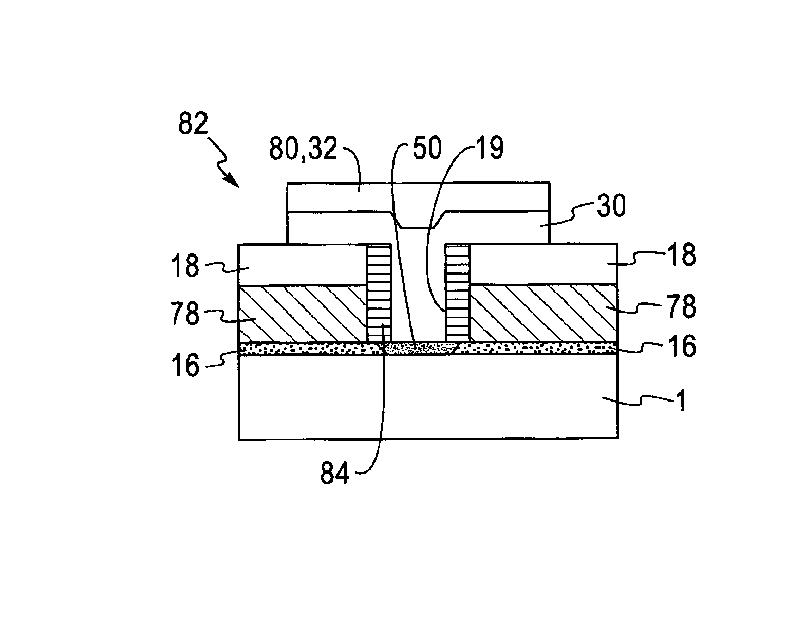
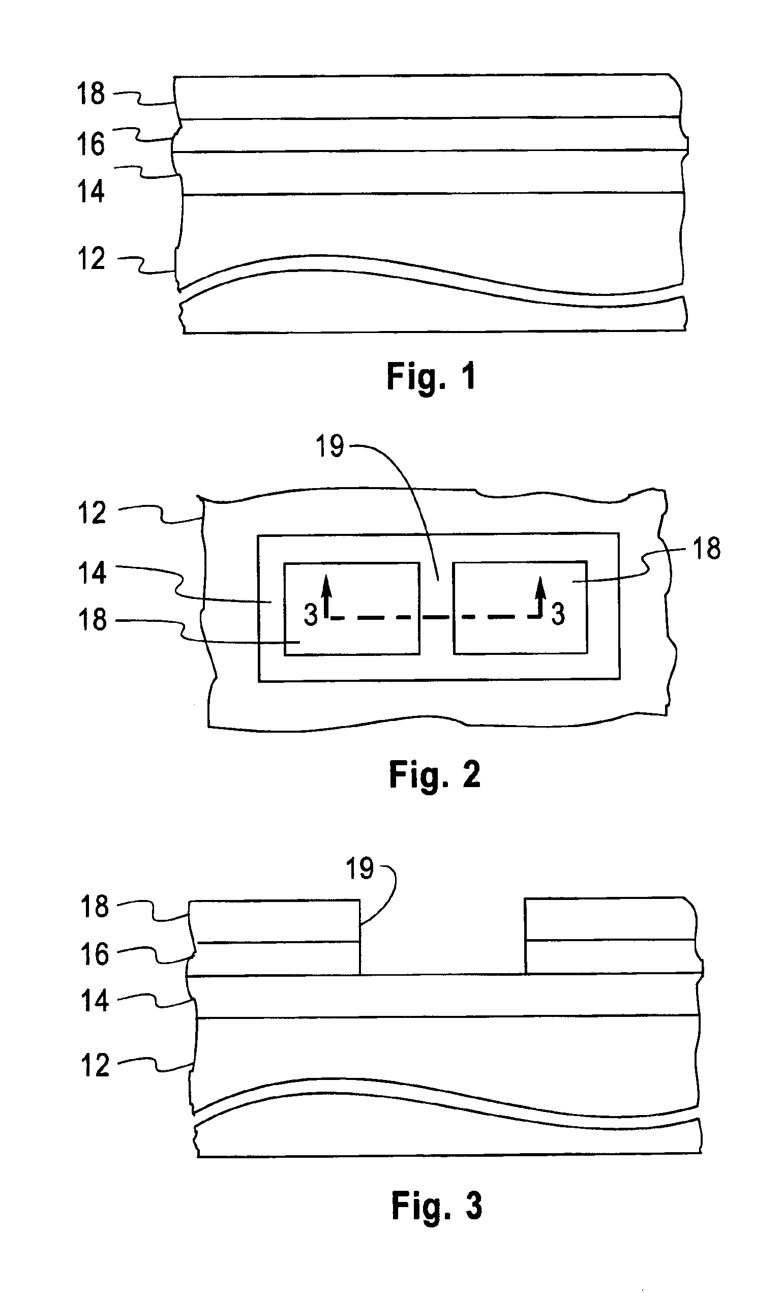
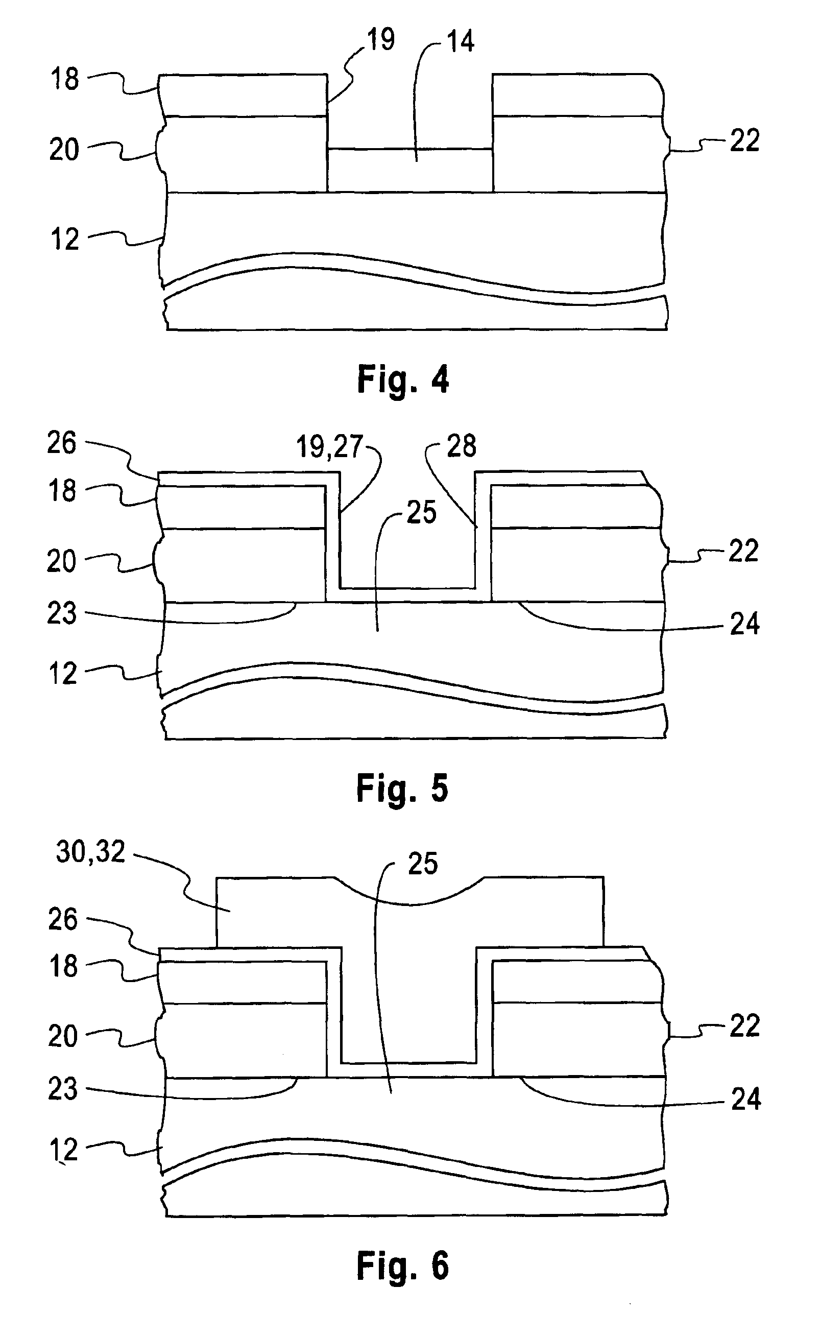
Referring now to the drawing, FIG. 1 shows a cross section view of substrate 12, a sacrificial layer 14, a metal layer 16 which subsequently forms a Schottky barrier or junction with respect to the channel, and an insulating layer 18. Substrate 12 may be a single crystal semiconductor material suitable to form the channel of a MOS FET to be built. Substrate 12 may be, for example, silicon, silicon germanium, germanium, gallium arsenide, indium gallium arsenide, indium phosphide, and indium gallium arsenide phosphide. Sacrificial layer 14 is of a material which may be selectively etched with respect to substrate 12 and which may be consumed by Schottky metal layer 16, for example, in the form of a silicide or germanide. Sacrificial layer 14 functions to protect the channel from reactive ion etching (RIE) damage. Sacrificial layer 14 may be for example silicon germanium with a germanium content x where x is equal to or greater than 0.3 and the silicon content is 1-x. Sacrificial layer...


PUM


Abstract

A field effect transistor and method for making is described incorporating self aligned source and drain contacts with Schottky metal-to-semiconductor junction and a T-shaped gate or incorporating highly doped semiconductor material for the source and drain contacts different from the channel material to provide etch selectivity and a T-shaped gate or incorporating a metal for the source and drain contacts and the oxide of the metal for the gate dielectric which is self aligned.

Description

FIELD OF THE INVENTIONThis invention relates to semiconductors and more particularly to self aligned metal oxide semiconductor (MOS) field effect transistors (FET's) having submicron gate lengths with a T-shaped gate.BACKGROUND OF THE INVENTIONState-of-the-art metal-oxide-semiconductor field effect transistors require shrinking the gate length below 0.25 μm. The standard process for forming the gates is by depositing a polysilicon layer, etching this layer to define the required gate length, and using the polysilicon as a mask for the source / drain shallow implant step. The shallow implant step is followed by forming a nitride sidewall spacer, implanting the deep ohmic region in the source / drain and then forming a metal silicide to the gate and the source / drain implant. The resistance of the gate thus increases as the gate length is reduced, because the gate metal silicide has the same gate length as the polysilicon gate underneath. The gate resistance slows down the devices because ...

Claims


Application Information

Patent Timeline
Patent Type & Authority Patents(United States)
IPC IPC(8): H01L27/085H01L27/095
CPCH01L27/095
Inventor CHAN, KEVIN KOKCHU, JACK OONISMAIL, KHALID EZZELDINRISHTON, STEPHEN ANTHONYSAENGER, KATHERINE LYNN
Owner IBM CORP
Why Eureka
Try Eureka