Semiconductor device using low dielectric constant material film and method of fabricating the same

a technology of dielectric constant and material film, which is applied in the direction of semiconductor devices, semiconductor/solid-state device details, electrical apparatus, etc., can solve the problems of inability to raise the integration scale, the fabrication cost is higher, and the conventional technique is unable to realize it easily, so as to achieve no restriction on the integration scale

Inactive Publication Date: 2006-08-15
RAMBUS INC
View PDF6 Cites 9 Cited by
  • Summary
  • Abstract
  • Description
  • Claims
  • Application Information

AI Technical Summary

Benefits of technology

[0008]Accordingly, an object of the present invention is to provide a semiconductor device that makes it possible to cope with the operating frequency in the order of GHz at a reasonable cost and that produces no restriction on the integration scale, and a method of fabricating the device.

Problems solved by technology

However, if the operating frequency enters the order of GHz, these conventional techniques are unable to realize it easily.
This is because signal transmission delay induced by the parasitic resistance and parasitic capacitance of the single-crystal silicon substrate itself is elicited.
If so, however, there arises another problem that the fabrication cost is higher, the integration scale is unable to be raised, and so on.

Method used


Image

  • Semiconductor device using low dielectric constant material film and method of fabricating the same
  • Semiconductor device using low dielectric constant material film and method of fabricating the same
  • Semiconductor device using low dielectric constant material film and method of fabricating the same

Examples


first embodiment

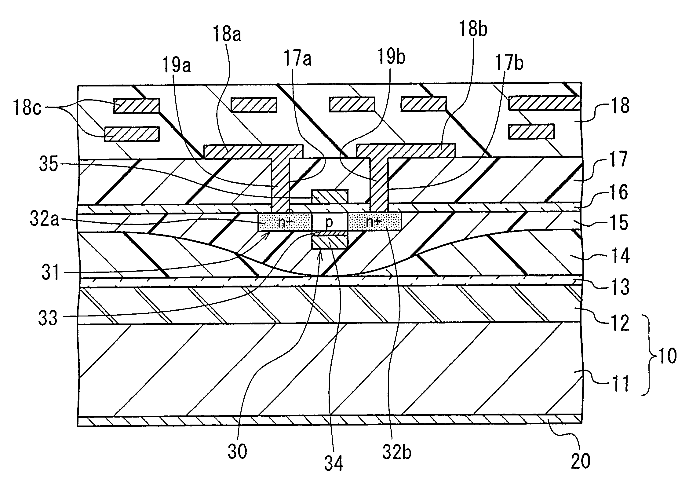
[0073]FIG. 1 is a cross-sectional view showing the configuration of a main part of a semiconductor device according to a first embodiment of the invention.

[0074]As shown in FIG. 1, the semiconductor device according to the first embodiment comprises a substrate 11, and a low dielectric constant material film 12 formed on the substrate 11. The substrate 11 and the film 12 constitute a base 10. The base 10 has such rigidity as to support the multilayer structure formed thereon. The surface of the film 12 forms the first surface of the base 10. The second surface of the base 10 is formed by the back surface of the base 11.

[0075]A semiconductor element layer including a MOS transistor 30 is fixed on the first surface of the base 10, i.e., on the surface of the low dielectric constant material film 12, with an adhesive film 13. The semiconductor element layer is constituted by the MOS transistor 30, interlayer insulator films 14 and 15, and insulator films 16 and 17. Further, a multilaye...

second embodiment

[0122]FIG. 9 is a cross-sectional view showing the configuration of a main part of a semiconductor device according to a second embodiment of the invention.

[0123]The semiconductor device of FIG. 9 corresponds to one obtained by adding a multilayer wiring structure 51 to the semiconductor device according to the first embodiment. Therefore, by attaching the same reference symbols as used for the device of the first embodiment to the same or corresponding elements in FIG. 9, detailed explanation about them is omitted here.

[0124]As shown in FIG. 9, the multilayer wiring structure 51 is provided between the low dielectric constant material film 12 forming the base 10, and the interlayer insulator film 14, in other words, the structure 51 is located between the base 10 and the semiconductor element layer. The source / drain region 32a of the transistor 30 in the semiconductor element layer is electrically connected to the predetermined wiring of the structure 51. The structure 51 is adhere...

third embodiment

[0133]FIG. 12 is a cross-sectional view showing the configuration of a main part of a semiconductor device according to a third embodiment of the invention.

[0134]The semiconductor device of FIG. 12 corresponds to one obtained by omitting the second gate electrode 35 of the MOS transistor 30 from the semiconductor device according to the first embodiment. Thus, by attaching the same reference symbols as used for the device of the first embodiment to the same or corresponding elements in FIG. 12, detailed explanation about them is omitted here.

[0135]Since the semiconductor device according to the third embodiment of the invention has substantially the same configuration as the device according to the first embodiment and therefore, it is apparent that the same advantages as those in the first embodiment are obtained.

[0136]Additionally, with the device of the third embodiment, the transistor 30 do not have the second gate electrode 35. Thus, there is an advantage that the configuration...


PUM


Abstract

The semiconductor device is capable of coping with speedup of operation using a low dielectric constant material film other than silicon. The base (10) formed by the substrate (11) and the low dielectric constant material film (12) whose relative dielectric constant is lower than silicon is provided. The semiconductor element layer including the MOS transistor (30) is adhered onto the surface of the base (10) for stacking. The transistor (30) is formed by using the island-shaped single-crystal Si film (31) and buried in the insulator films (15), (16) and (17). The multilayer wiring structure (18) is formed on the semiconductor element layer and is electrically connected to the transistor (30). The electrode (20) functioning as a return path for the signals is formed on the back surface of the base (10). Instead of forming the electrode (20) on the base (10), the electrodes (20A) may be arranged on the back surface of the base (10A), configuring the base (10A) as an interposer.

Description

[0001]This is a National Phase Application in the United States of International Patent Application No. PCT / JP02 / 11494 filed Nov. 5, 2002, which claims priority on Japanese Patent Application No. 2001-340076, filed Nov. 5, 2001. The entire disclosures of the above patent applications are hereby incorporated by reference.TECHNICAL FIELD[0002]The present invention relates to a semiconductor device and a method of fabricating the same and more particularly, to a semiconductor device using a base including a low dielectric constant material film whose relative dielectric constant is lower than silicon (Si) to raise its operation speed, and a method of fabricating the device.BACKGROUND ART[0003]Conventionally, as one of the techniques coping with the miniaturization and higher integration of semiconductor elements mounted on a semiconductor device, the SOI (Silicon On Insulator) technique has been known. This technique is a technique for forming a single-crystal silicon film on an insula...

Claims


Application Information

Patent Timeline
Patent Type & Authority Patents(United States)
IPC IPC(8): H01L29/80H01L21/336H01L21/822H01L21/84H01L27/06H01L27/12H01L29/423H01L29/786
CPCH01L21/8221H01L21/84H01L27/0688H01L29/78648H01L29/42384H01L29/66772H01L29/78603H01L27/12H01L2224/2919H01L2224/32145H01L23/485H01L2924/00014H01L21/31H01L21/76898
Inventor KOYANAGI, MITSUMASA
Owner RAMBUS INC
Why Eureka
Try Eureka