Static random access memory

a random access memory and random access technology, applied in static storage, digital storage, instruments, etc., can solve the problems of low-performance mos transistors in latches, low-performance devices for fast flipping during write operation, and failure of flipping, so as to reduce the operation cycle time and fast access time , the effect of low power consumption

Inactive Publication Date: 2007-09-20
KIM JUHAN
View PDF0 Cites 11 Cited by
  • Summary
  • Abstract
  • Description
  • Claims
  • Application Information

AI Technical Summary

Benefits of technology

[0017] The memory cells can be formed within the current CMOS process environment, but with no new material. Thus, the peripheral circuits and the memory cells can be formed on the conventional wafer, such as the bulk wafer and the SOI wafer. Furthermore, one of major improvement of the present invention is that the memory cells can be formed in between the routing layers in order to reduce chip area, and also the memory cells can be stacked over the control circuits including MOS transistors where the memory cells are composed of the thin-film transistor such as polysilicon and amorphous silicon with low temperature process. The read diode need not be a high performance device nor have a high current gain, because the current path of diode includes its whole junction area while the current path of MOS transistor includes a shallow inversion layer on the surface by the electric field. Thus, the current gain of the diode is much higher than that of the MOS transistor. The write MOS transistor need not be a high performance device nor have a high current gain either. During write, the write MOS transistor drives only a small storage inverter only, which means that the write MOS device can be a coarse MOS transistor, such as polysilicon or amorphous thin-film MOS transistor. In this manner, the coarse MOS transistor serves as a good write device. In addition, multiple memory cells can be stacked. Hence, topping the memory cells with low temperature is independent on fabricating the control circuits.
[0018] The heavily loaded lines are driven by the bipolar output drivers, and the MOS transistor drive only lightly loaded signals. This means that the control circuits can be stacked over the wafer with an insulator because there is no need for fabricating high-performance MOS transistor on the surface of the wafer, where the strong bipolar buffers also formed from the thin-film layers. In doing so, the wafer only serves as a supporter while the conventional MOS transistors use the surface of the wafer, which means that the MOS transistors for the memory control and the memory cells are formed from the deposited polysilicon or amorphous silicon. Thus, any types of wafer can be a supporter in order to reduce the wafer cost. In this respect, there is no need of extreme feature size transistors because the memory cells can be stacked over the control circuit, and the control circuits can be stacked over the any type of wafer. In stead of scaling the transistors, multiple toppings are more meaningful, which also achieves fast access with centralized control and short routing length in vertical directions. In doing so, the present invention can overcome the scaling limit of the SRAM, because there is almost no limit to stack the memory cells in the vertical direction as long as the flatness is good enough to stack more memory cells.
[0021] However the operation of the four-terminal diode is not familiar with the memory operation, because it has unidirectional current control characteristic and internal feedback loop, even though it has almost no parasitic effect. In the present invention, sophisticated circuit techniques are introduced to use a diode as a read access device for the SRAM operation. Moreover, the diode serves as a sense amplifier to detect the voltage of the storage node whether it is forward bias or not, then diode sends binary results to the bit line, and the latch device including the current mirror receives the binary results from the bit line, on or off. The current mirror repeats the amount of current that the memory cell flows, and latches the result. After latching data, the output of the latch device cuts off the current path of the bit line, which reduces active current. And the diode read device realizes fast access time, and does not require reference bit line. Furthermore, dummy cells generate replica delay signals which guarantee internal timing margin and reduce operation cycle time. Furthermore, the diode can flow more current than the MOS transistor. The word line cuts off the holding current during standby. Thus there is no standby current except leakage current, which realizes low power consumption. Furthermore, the applications of the present memory cell are extendable for multi port memory and content addressable memory.

Problems solved by technology

However, fabricating the MOS transistor will be reached to the scaling limit in the near future, and also the process cost will be extremely expensive with smaller feature size, such 45 nm, 32 nm and 22 nm.
Thus, six MOS transistors are used to configure a memory cell, which is the major drawback of the conventional SRAM because it occupies relatively wider area than other types of memories, such as DRAM.
In order to achieve fast read operation, all six MOS transistors should be high-performance devices, but the MOS transistors in the latch should be low-performance device for fast flipping during write operation, because the latch should be flipped by the bit lines.
When the MOS transistors of the latch are too strong, the flipping is very slow or failed, while the read operation is relatively fast.
And one more major drawback is that fabricating the high-performance MOS transistor on the surface of the wafer reaches to the scaling limit in the near future, such that smaller than 22 nm MOS transistor is more challenging with the existing materials and less economical.
However, the bi-directional traffic is generally slow.
However the diode operation is not as simple as the MOS transistor because it has unidirectional current control characteristic and internal feedback loop.
Conversely, using diode as a read access device gives the bit line loading to the read word line through the diode, which makes the read word line loading very heavy, but it is controllable to design with strong driver or segmentation for the read word line.

Method used


Image

  • Static random access memory
  • Static random access memory
  • Static random access memory

Examples


Embodiment Construction

)

[0046] Reference is made in detail to the preferred embodiments of the invention. While the invention is described in conjunction with the preferred embodiments, the invention is not intended to be limited by these preferred embodiments. On the contrary, the invention is intended to cover alternatives, modifications and equivalents, which may be included within the spirit and scope of the invention as defined by the appended claims. Furthermore, in the following detailed description of the invention, numerous specific details are set forth in order to provide a thorough understanding of the invention. However, as is obvious to one ordinarily skilled in the art, the invention may be practiced without these specific details. In other instances, well-known methods, procedures, components, and circuits have not been described in detail so that aspects of the invention will not be obscured.

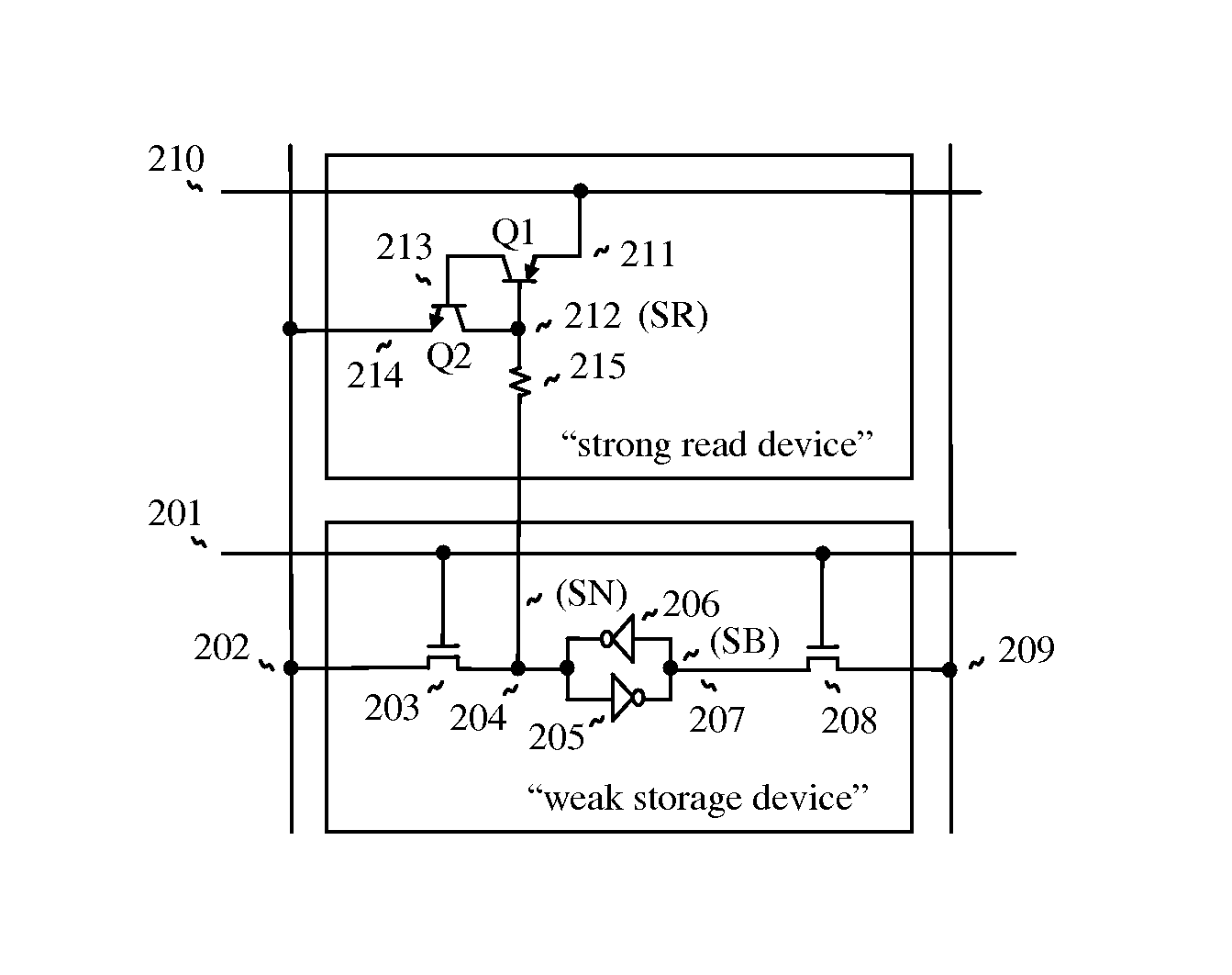
[0047] The present invention is directed to a static random access memory, as shown in FIG. 2. Th...


PUM


Abstract

SRAM cell includes a four-terminal diode as a read device wherein the first terminal is connected to a read word line, the second terminal is connected to a storage device through a resistor, the third terminal is floating, and the fourth terminal is connected to one of two bit lines; and two MOS transistors as a write device; and each MOS transistor is connected to the bit line respectively; and a latch including two cross-coupled inverters as the storage device; and the SRAM cell can be formed from thin-film layer, thus multiple memory cells are stacked; and the heavy routing lines are driven by the bipolar drivers which are part of the invention, hence the bipolar circuits and the control MOS transistors of the peripheral circuit can be formed from the deposited thin-film layers; consequently the whole chip can be stacked over the wafer, such as silicon, quartz and others; additionally it applications are extended to a multi port memory and a content addressable memory.

Description

CROSS REFERENCE TO RELATED APPLICATION [0001] The present invention is a continuation of application Ser. No. 11 / 755,197, filed on May 30, 2007, which is a continuation of application Ser. No. 11 / 164,919, filed on Dec. 11, 2005, now U.S. Pat. No. 7,196,926, which are herein incorporated by reference.FIELD OF THE INVENTION [0002] The present invention relates generally to integrated circuits, in particular to SRAM (Static Random Access Memory) including a static storage element, and its applications, such as single port memory, multi port memory and CAM (content addressable memory). BACKGROUND OF THE INVENTION [0003] A p-n-p-n diode known as Shockley diode or thyristor, is a solid-state semiconductor device similar to two-terminal p-n diode, with an extra terminal which is used to turn it on. Once turned on, diode (p-n-p-n diode or n-p-n-p diode) will remain on conducting state as long as there is a significant current flowing through it. If the current falls to zero, the device swit...

Claims


Application Information

Patent Timeline
Patent Type & Authority Applications(United States)
IPC IPC(8): G11C16/06
CPCG11C11/412G11C8/16G11C15/04
Inventor KIM, JUHAN
Owner KIM JUHAN
Why Eureka
Try Eureka