

Method of manufacturing semiconductor package having multiple rows of leads
a manufacturing method and lead frame technology, applied in the direction of electrical apparatus construction details, casings/cabinets/drawers, electrical apparatus details, etc., can solve the problems of increased manufacturing costs, difficult individualization process (as a post packaging process), and damage to the coherence of the bonding surface between the molding material and the lead frame, so as to achieve reliable semiconductor packages, reduce manufacturing costs, and enhance the planarity of leads
- Summary
- Abstract
- Description
- Claims
- Application Information
AI Technical Summary
Benefits of technology
Problems solved by technology
Method used
Image

Examples
Embodiment Construction
[0023] Hereinafter, the present invention is described more in details with reference to the accompanying drawings, in which exemplary embodiments of the invention are shown.
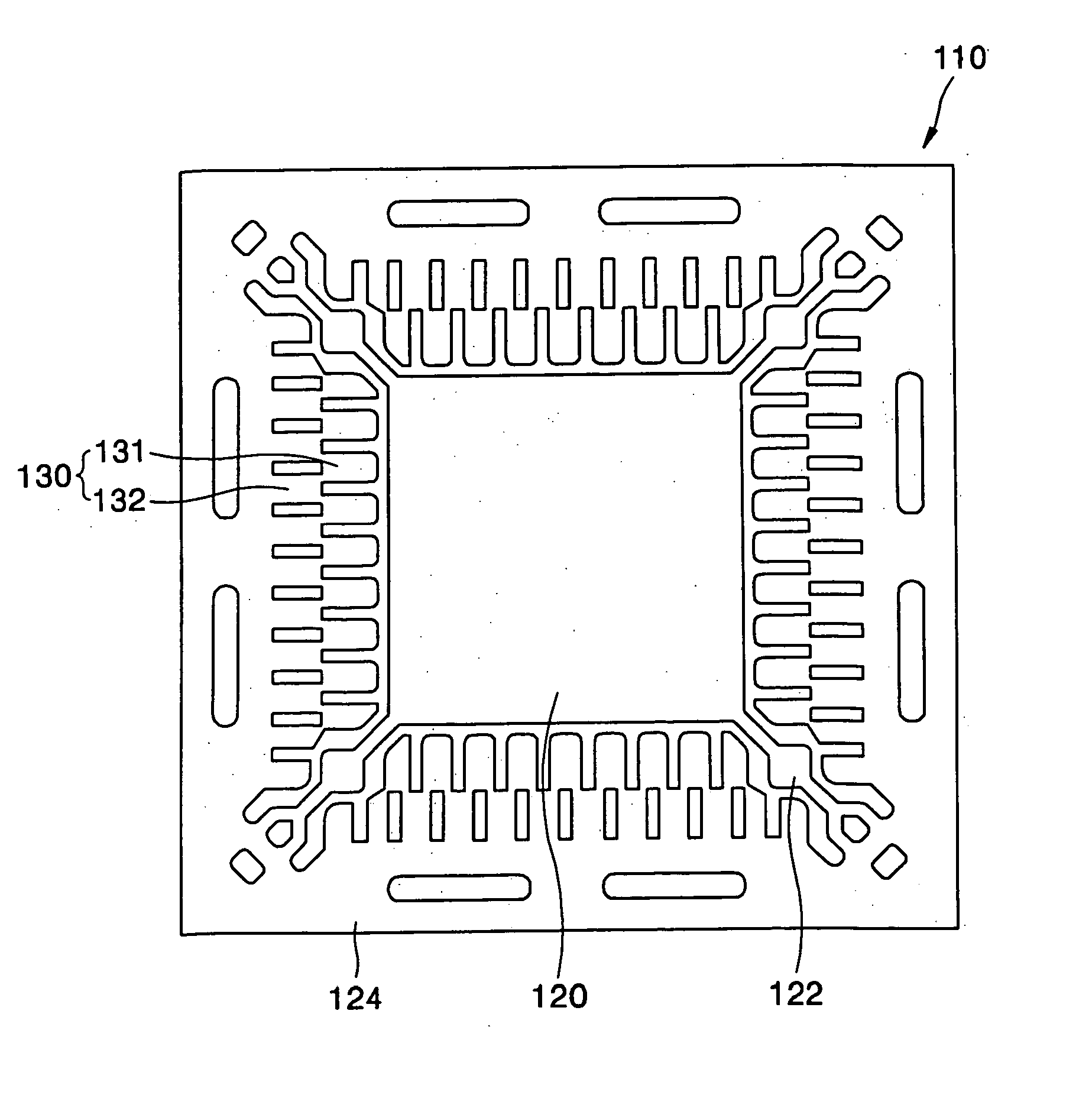
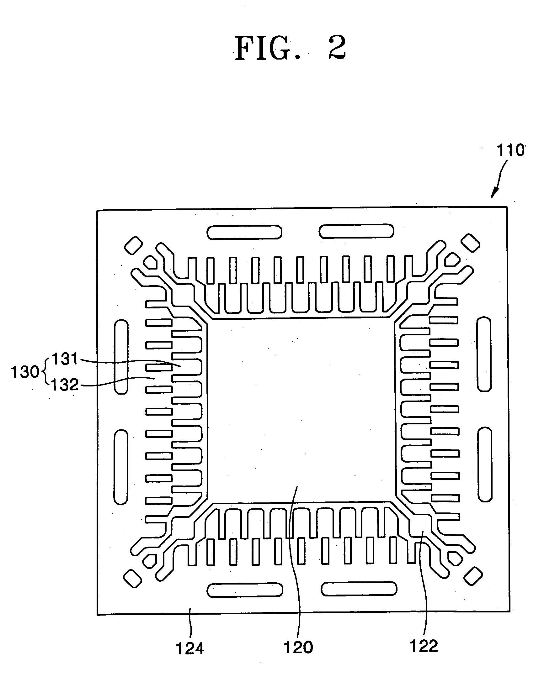
[0024]FIG. 2 shows an example of a lead frame for a semiconductor package, which includes two rows of leads. The lead frame includes a die pad 120 configured to mount a semiconductor chip thereon, and two rows of leads 130 arranged about the die pad 120. The die pad 120 is connected to an outer flame 124 by a pad supporter (a so-called tie bar) 122 and supports the semiconductor chip thereon.
[0025] The leads 130 include first rows of leads 131 and second rows of leads 132, each of the leads adapted to electrically connect the semiconductor chip to an external substrate (e.g., a PCB) as an input / output terminal. When an assembly process of the semiconductor package is completed, the outer frame 124 is to be removed.
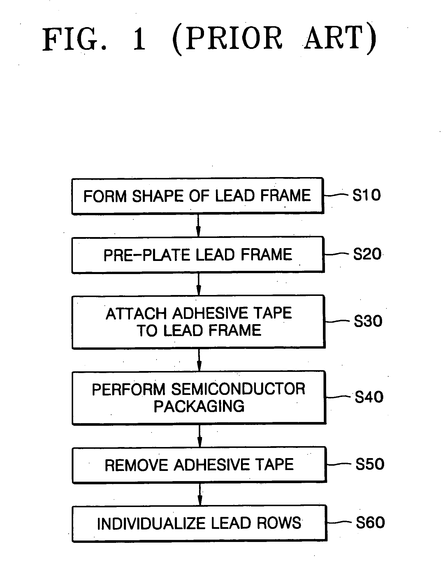
[0026]FIG. 3 is a flowchart illustrating a method of manufacturing a semiconductor package havin...
PUM
 Abstract
Description
Claims
Application Information