Electronic device and method of manufacturing the same

a technology of electronic devices and manufacturing methods, applied in the direction of semiconductor devices, electrical apparatus, transistors, etc., can solve the problems of voids, polycrystalline grains agglomeration, and inability to operate at high speed in the channel region, so as to facilitate heat exhaustion, improve the uniformity of polycrystalline grains, and improve the effect of thermal conductive layer

Inactive Publication Date: 2005-10-27
SAMSUNG ELECTRONICS CO LTD
View PDF10 Cites 9 Cited by
  • Summary
  • Abstract
  • Description
  • Claims
  • Application Information

AI Technical Summary

Benefits of technology

[0012] Embodiments of the present invention provide an electronic device including a polysilicon layer consisting of improved uniformity of polycrystalline grains, which is acquired by interposing a high thermal conductive layer between a plastic substrate and an amorphous silicon layer so as to facilitate heat exhaust during crystallization of the amorphous silicon.

Problems solved by technology

However, the channel region cannot operate at high speed due to low carrier mobility.
However, the foregoing crystallization methods cause agglomeration of polycrystalline grains, voids produced between the polycrystalline grains, and a poor surface roughness.

Method used


Image

  • Electronic device and method of manufacturing the same
  • Electronic device and method of manufacturing the same
  • Electronic device and method of manufacturing the same

Examples


Embodiment Construction

[0034] The present invention will now be described more fully with reference to the accompanying drawings, in which exemplary embodiments of the invention are shown. The thicknesses of layers or regions in the drawings are exaggerated for clarity. The same reference numerals are used to denote the same elements throughout the drawings.

[0035] At the outset, a thin film transistor (TFT) according to embodiments of the present invention will be described.

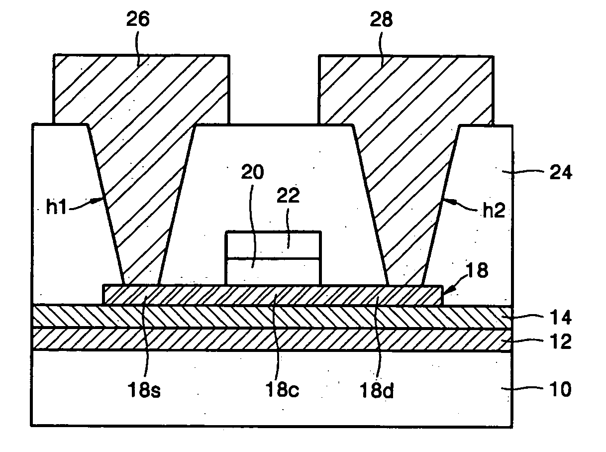
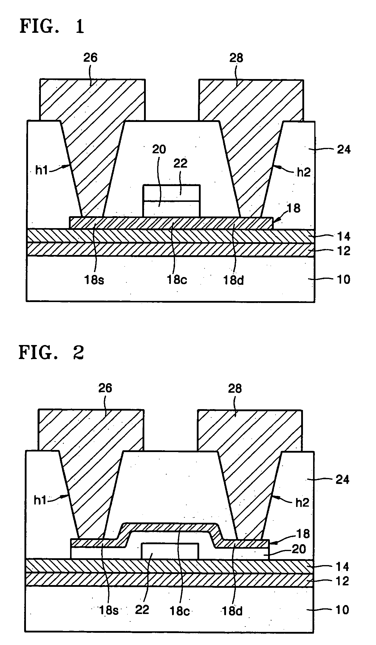
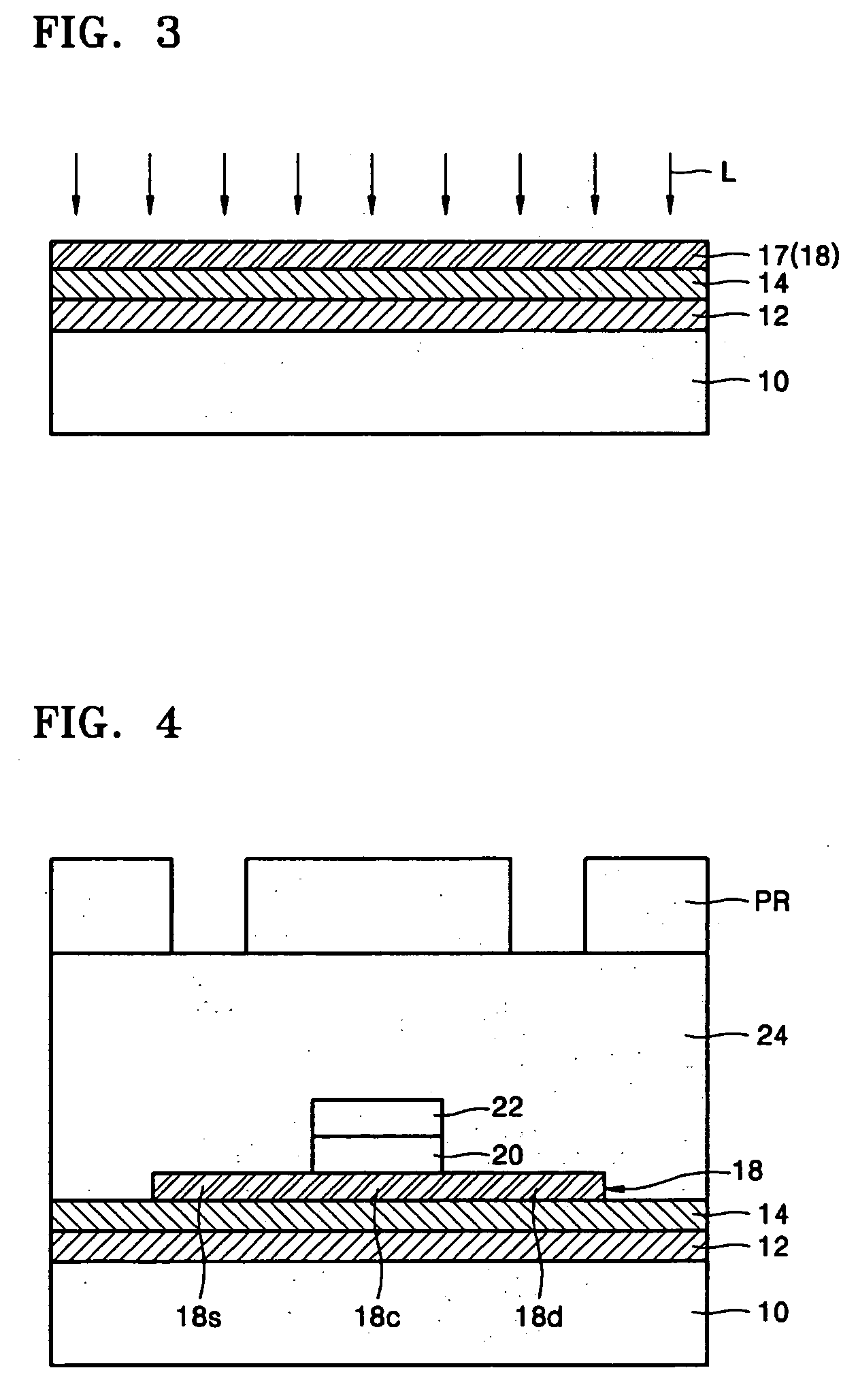
[0036]FIG. 1 is a cross-sectional view of a top gate type TFT according to an embodiment of the present invention.

[0037] Referring to FIG. 1, a thermal conductive layer 12 and a buffer layer 14 are sequentially stacked on a substrate 10. The thermal conductive layer 12 has a predetermined thickness of, for example, about 1000 Å, and a high thermal conductivity. The buffer layer 14 has a predetermined thickness of 2000 Å. The substrate 10 is a plastic substrate.

[0038] If the thermal conductive layer 12 is an insulating layer formed ...


PUM


Abstract

Provided are an electronic device and a method of manufacturing the same. The device includes a plastic substrate, a transparent thermal conductive layer stacked on the plastic substrate, a polysilicon layer stacked on the thermal conductive layer; and a functional device disposed on the polysilicon layer. The functional device is any one of a transistor, a light emitting device, and a memory device. The functional device may be a thin film transistor including a gate stack stacked on the polysilicon layer.

Description

BACKGROUND OF THE INVENTION [0001] Priority is claimed to Korean Patent Application No. 10-2004-0024010, filed on Apr. 8, 2004 in the Korean Intellectual Property Office, the disclosure of which is incorporated herein in its entirety by reference. [0002] 1. Field of the Invention [0003] The present invention relates to an electronic device and a method of manufacturing the same. [0004] 2. Description of the Related Art [0005] A flat panel display (FPD), such as an organic light emitting diode (OLED) display or a liquid crystal display (LCD), employs a thin film transistor (TFT) as a switching device. A channel region of the TFT can be formed of amorphous silicon (a-Si) or polysilicon. [0006] If the channel region of the TFT is formed of a-Si, a uniform layer can be formed at a relatively low temperature. However, the channel region cannot operate at high speed due to low carrier mobility. [0007] If the channel region of the TFT is formed of polysilicon, carrier mobility can be incre...

Claims


Application Information

Patent Timeline
Patent Type & Authority Applications(United States)
IPC IPC(8): H01L21/20H01L21/336H01L21/84H01L27/12H01L29/786
CPCH01L29/66757H01L29/66765H01L29/78678H01L29/78675H01L29/78603A47J36/06
Inventor JUNG, JI-SIMNOGUCHI, TAKASHICHO, HANS S.KIM, DO-YOUNGPARK, KYUNG-BAE
Owner SAMSUNG ELECTRONICS CO LTD
Why Eureka
Try Eureka