Wafer stabilization device and associated production method

a stabilizing device and stabilizing technology, applied in the direction of semiconductor devices, electrical equipment, basic electric elements, etc., can solve the problems of unstable and warped wafers not being processed in a standardized unit, inability to work with automatic handling systems, and thin wafers being produced. , to achieve the effect of avoiding deformation of thin wafers

Inactive Publication Date: 2005-10-27
INFINEON TECH AG
View PDF13 Cites 42 Cited by
  • Summary
  • Abstract
  • Description
  • Claims
  • Application Information

AI Technical Summary

Benefits of technology

[0007] In one embodiment, unstable and distorted thin wafers can be processed and handled securely in terms of production in processing processes and also, upstream and downstream, on transport paths. A stabilization device in the form of a carrier system which fixedly holds the thin wafer and orients it in planar fashion is used. The function of such a carrier system is ensured by a stiff profile, which is arranged at the peripheral region of the thin wafer on at least one of its parallel surfaces and is intimately connected thereto. In order to eliminate deformation of the thin wafer, the thin wafer is shaped by the external force applied by means of the device such that thin wafer assumes a planar shape and also retains the planar shape during the subsequent processes.
[0010] The basic body of a carrier described is produced from material having an expansion coefficient that is identical or similar to that of the wafer. This ensures that it is intrinsically stable given a sufficient thickness, can sufficiently support the wafer, can be used even in aggressive environments, and stresses between the carrier and the wafer do not occur or are minimized in the event of temperature fluctuations.

Problems solved by technology

Furthermore, as the mechanical instability increases, the more thinly the wafer is produced.
In the process steps provided for the wafer, deformations and instabilities of this type mean that it is difficult, if not impossible to work with automatic handling systems at present as in many cases, such an unstable and warped wafer cannot be processed in a standardized unit.
The problem of instability and distortion has occurred to an increased extent with the use of extremely thin wafers.
A further decrease in the layer thickness of wafers in the future may give rise to even greater problems.
This wafer instability has the effect that previous handling systems for thin wafers fail and the rejects in the course of production are comparatively high.

Method used


Image

  • Wafer stabilization device and associated production method
  • Wafer stabilization device and associated production method
  • Wafer stabilization device and associated production method

Examples


Embodiment Construction

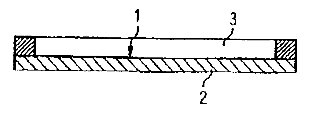
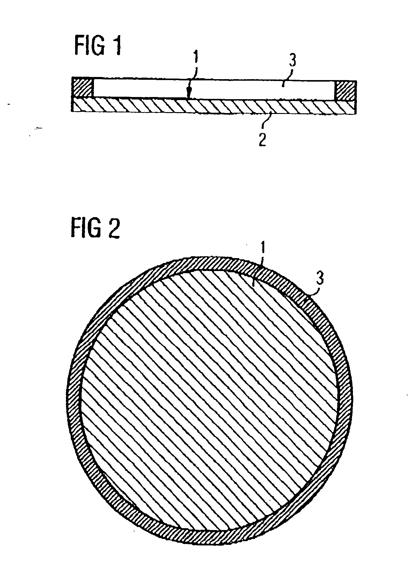
[0020] A composite 1 is illustrated in FIG. 1. The composite 1 comprises a thin wafer 2 and a stabilization device in the form of a carrier ring 3. The thin wafer 2 and carrier ring 3 are intimately connected to one another such that the thin wafer 2 bears on the carrier ring 3 in a planar and dimensionally stable manner and can be handled and also processed.

[0021] The geometry of the carrier ring 3 for the thin wafer 2 may be designed in different ways. For example, if the processing of the thin wafer 2 takes place on both sides, the stabilization device is designed as a simple carrier ring 3 and receives a thin wafer 2, bearing areas in the form of an annulus being present only on the peripheral region of the wafer 2. This is illustrated in plan view in FIG. 2.

[0022] This structure precludes neither front-side nor rear side processing of the thin wafer 2, so that the thin wafer 2 can be processed on both sides. The carrier ring 3 is designed such that the bearing areas of the ca...


PUM


Abstract

A stabilization device and method for stabilizing a workpiece such as a thin film wafer is presented. The thin wafer is fixed and oriented in planar fashion. The stabilization device is realized by a profiled ring which is arranged on the periphery of the wafer and is intimately connected thereto. The stabilization device and wafer are connected via negative pressure or by means of an adhesive having high thermal stability. The wafer and device are formed from similar semiconductor materials and have the same outline contour. The stabilization device remains on the wafer during process steps in the course of production and processing of the wafer.

Description

PRIORITY [0001] This application claims the benefit of priority to German Patent Application 10 2004 018 250.7, filed on Apr. 15, 2004, herein incorporated by reference in its entirety. TECHNICAL FIELD [0002] The invention relates to a device for stabilizing a workpiece, in particular a thin wafer, which is fixed and oriented in planar fashion, and to a method for producing this device. BACKGROUND [0003] Semiconductor materials in the form of wafers are used for producing electronic components. Integrated circuits are produced on such a disk in processing stations and production lines. For this purpose, a wafer is transported step by step from one production unit to the next. The identification, fixing and relative orientation of the wafer with respect to each processing unit are significant in this case. [0004] Wafers having a larger diameter are increasingly being used in the course of technical developments; diameters of 5 to 6 inches can be produced as standard and diameters of ...

Claims


Application Information

Patent Timeline
Patent Type & Authority Applications(United States)
IPC IPC(8): H01L21/46H01L21/68H01L21/687H01L29/06
CPCH01L21/6835H01L21/6836H01L2221/6834H01L2221/68327H01L21/68757
Inventor KRONINGER, WERNERSCHWAIGER, JOSEF
Owner INFINEON TECH AG
Why Eureka
Try Eureka