Self-emitting display

a display and self-emitting technology, applied in the field of flat panel displays, to achieve the effect of improving the manufacturing tolerance, improving the yield, and improving the performance characteristics and display quality of the resulting organic el display

Active Publication Date: 2005-10-27
SAMSUNG DISPLAY CO LTD +1
View PDF5 Cites 36 Cited by
  • Summary
  • Abstract
  • Description
  • Claims
  • Application Information

AI Technical Summary

Benefits of technology

[0028] 2. The displacement in the direction of θ is taken care of in the process of vapor-depositing a light-emitting layer, and thus the manufacturing tolerance is improved in the vapor deposition process in the organic EL display, favorably leading to better yield.
[0029] 3. Organic EL display can be easily increased in size.
[0030] 4. The varying widths of the signal line can control the signal voltage not to decrease that much, successfully leading to better performance characteristics and display quality of the resulting organic EL display.
[0031] 5. With higher accuracy at the time of vapor-depositing a light-emitting layer, the display can have higher definition, and with less signal voltage reduction from the peripheral portion of the screen to the center portion thereof, the screen can be uniform in display intensity.
[0032] This is applicable not only to the above organic EL displays of a low-molecular light-emitting material but also to organic EL displays of a high-molecular light-emitting material, or self-emitting displays of any other types, e.g., PDPs and FEDs, specifically to form electrodes and fluorescent bodies provided with electronic sources. With self-emitting displays, the manufacturing tolerance associated with screen size increase is dominantly controlled by the aperture design for the light-emitting portion. The design approach of the present invention applied to the aperture diameter is to increase the manufacturing tolerance, thereby enabling increasing the manufacturing tolerance of general flat panel displays.
[0033] Because the flat panel displays are made airtight and protected from the air, a signal line is provided from the peripheral portion of the screen (contour part of the flat panel display) for driving the display. Thus, the larger the size of the flat panel display, the longer the signal line will be, and thus the signal voltage is inevitably reduced. According to the present invention, on the other hand, by grading the width of the signal line, the signal voltage can be controlled not to decrease that much.

Problems solved by technology

In the case of forming a light-emitting layer by vapor deposition using such a vapor deposition mask, there arise problems associated with the following reasons.

Method used


Image

  • Self-emitting display
  • Self-emitting display
  • Self-emitting display

Examples


first embodiment

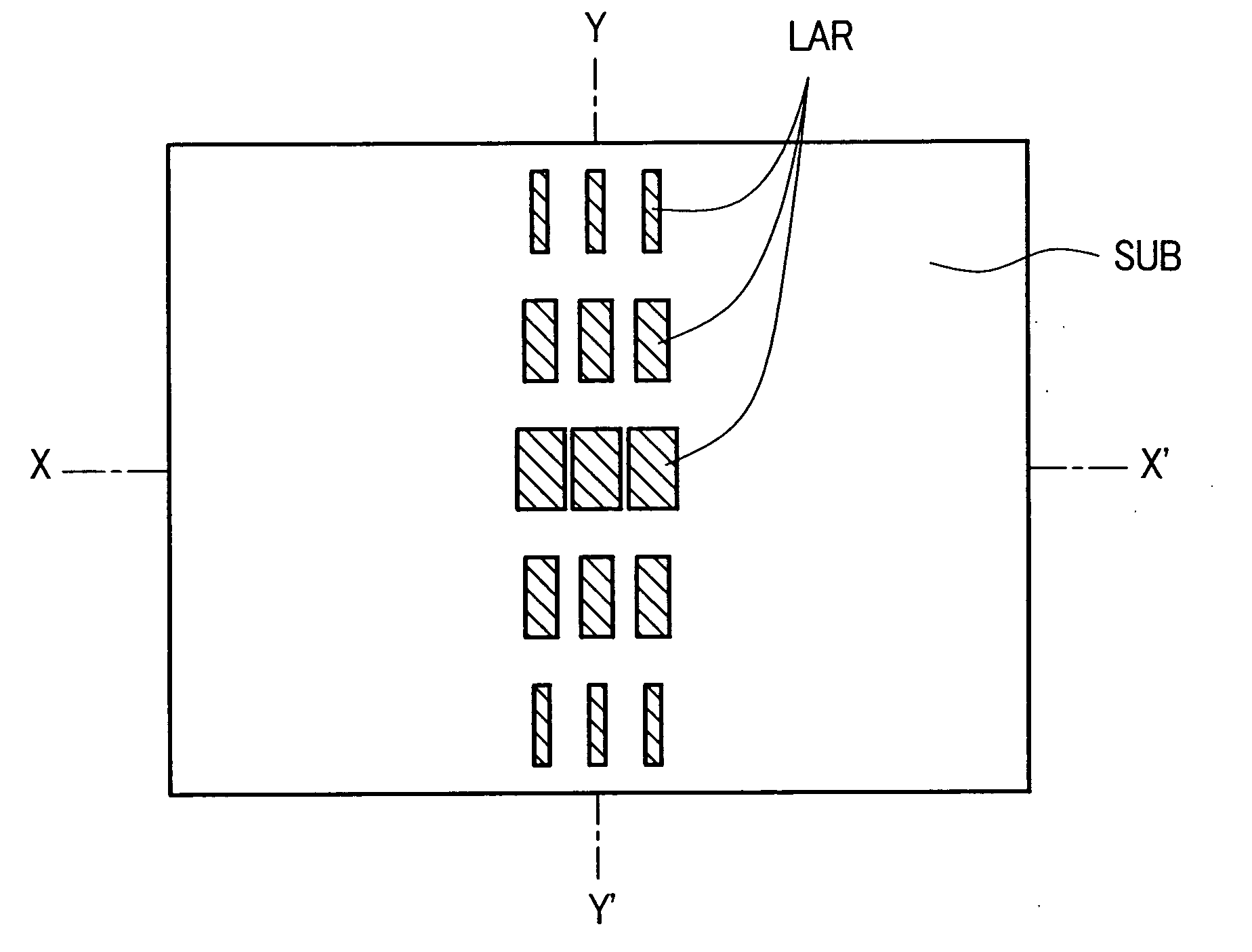
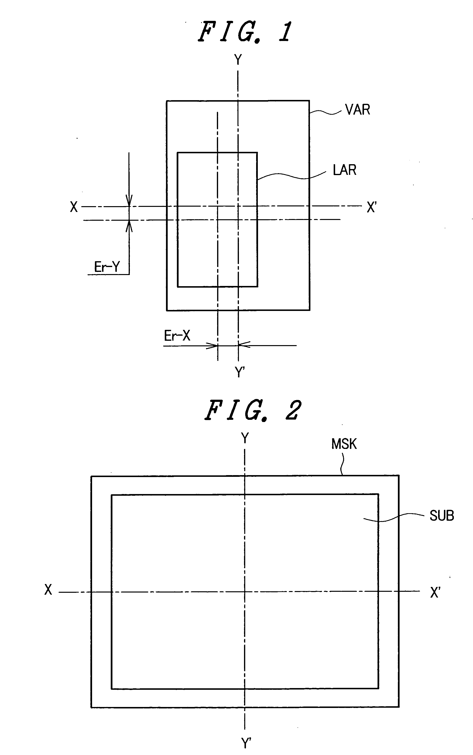
[0058]FIG. 9 is a schematic plan view of an aperture of a light-emitting portion illustrating a first embodiment of the present invention. Exemplarily shown here are only three aperture rows at the center portion of a screen in the direction of Y-Y′. The size of the aperture LAR is largest at the center portion of the screen, and the width in the direction of X is graded so as to be narrowed by degrees with distance therefrom in the direction of Y-Y′. FIG. 10 is a schematic plan view of a signal line illustrating the first embodiment of the present invention. Shown here is only a signal line (drive power line) CL extending in the direction of Y-Y′ at the center portion of the screen.

[0059] As shown in FIG. 10, the power line CL formed on the glass substrate SUB is narrow at the center portion, and increasing in width by degrees in the direction of X with distance therefrom in the direction of Y-Y′.

[0060] In the organic EL displays of the present embodiment, a yield of almost 100% ...


PUM

PropertyMeasurementUnit
widthaaaaaaaaaa
sizeaaaaaaaaaa
widthaaaaaaaaaa

Abstract

An aperture LAR of a light-emitting portion is changed in diameter (size) from the center portion of a screen to the peripheral portion thereof. In this manner, any displacement observed between the aperture LAR and a vapor deposition region VAR of an organic EL material is controlled. The aperture LAR is preferably larger in size at the center portion of the screen, and smaller in the peripheral portion thereof. As such, a light-emitting layer is vapor-deposited on a substrate correctly for every pixel so that a high-quality self-emitting display including organic EL display can de derived.

Description

CROSS-REFERENCE TO RELATED APPLICATIONS [0001] The disclosure of Japanese Patent Application No. 2004-113476 filed on Apr. 7, 2004 including the specification, drawings and abstract is incorporated herein by reference in its entirety. BACKGROUND OF THE INVENTION [0002] 1. Field of the Invention [0003] The present invention relates to flat panel displays and, more specifically, to a display suitably serving as a self-emitting display providing better positioning accuracy between a power supply line and pixels, and providing high-quality display by controlling the signal voltage not to decrease that much even if the wiring of the power supply line is increased in length. [0004] 2. Description of the Related Art [0005] Flat-panel self-emitting displays include plasma display panels (PDPs), field emission displays (FEDs), organic electroluminescence displays (organic EL displays, referred also to as OLEDs), and others, which are already commercially available or are currently underway f...

Claims


Application Information

Patent Timeline
Patent Type & Authority Applications(United States)
IPC IPC(8): C23C14/04H01L51/50G09F9/30H01L27/32H01L51/56H05B33/00H05B33/02H05B33/12H05B33/14
CPCH01L27/3244H01L51/56H01L27/3276H01L27/3246H10K59/122H10K59/12H10K59/131H10K71/00
Inventor MATSUDATE, NORIHARUSAKAMOTO, HIROTSUGU
Owner SAMSUNG DISPLAY CO LTD
Why Eureka
Try Eureka