Solid-state image sensor

a solid-state image sensor and image sensor technology, applied in the field can solve the problems of wide variations in photosensitivity and charge transfer characteristics, and the vulnerability of solid-state image sensors including 3-tr-pixels to noise caused by ktc noises

Inactive Publication Date: 2005-10-27
FUJITSU SEMICON LTD
View PDF6 Cites 63 Cited by
  • Summary
  • Abstract
  • Description
  • Claims
  • Application Information

AI Technical Summary

Benefits of technology

[0015] According to the present invention, the metal interconnection layers formed above the pixels can shield light almost equally among the pixels, whereby the light receiving characteristics can be uniform among the pixels.

Problems solved by technology

It is said that the solid-state image sensor including 3-Tr-pixels are vulnerable to noises (kTC noises) caused by thermal noises.
However, the proposed pixel layouts having a read transistor part made common between adjacent pixels causes wide variations in photosensitivities and charge transfer characteristics.

Method used


Image

  • Solid-state image sensor
  • Solid-state image sensor
  • Solid-state image sensor

Examples


first embodiment

A First Embodiment

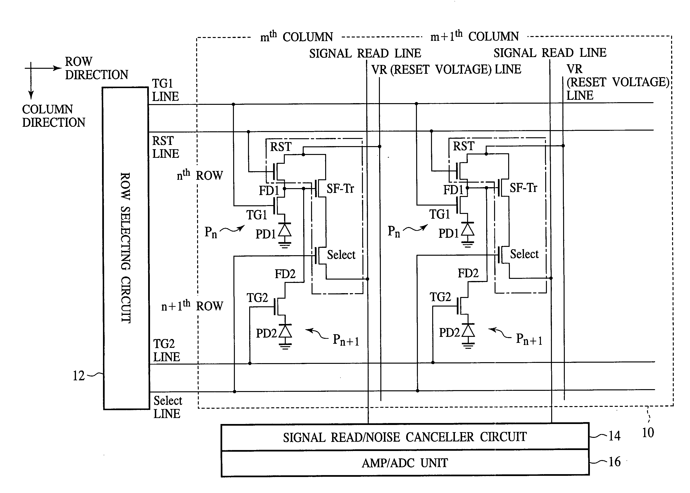
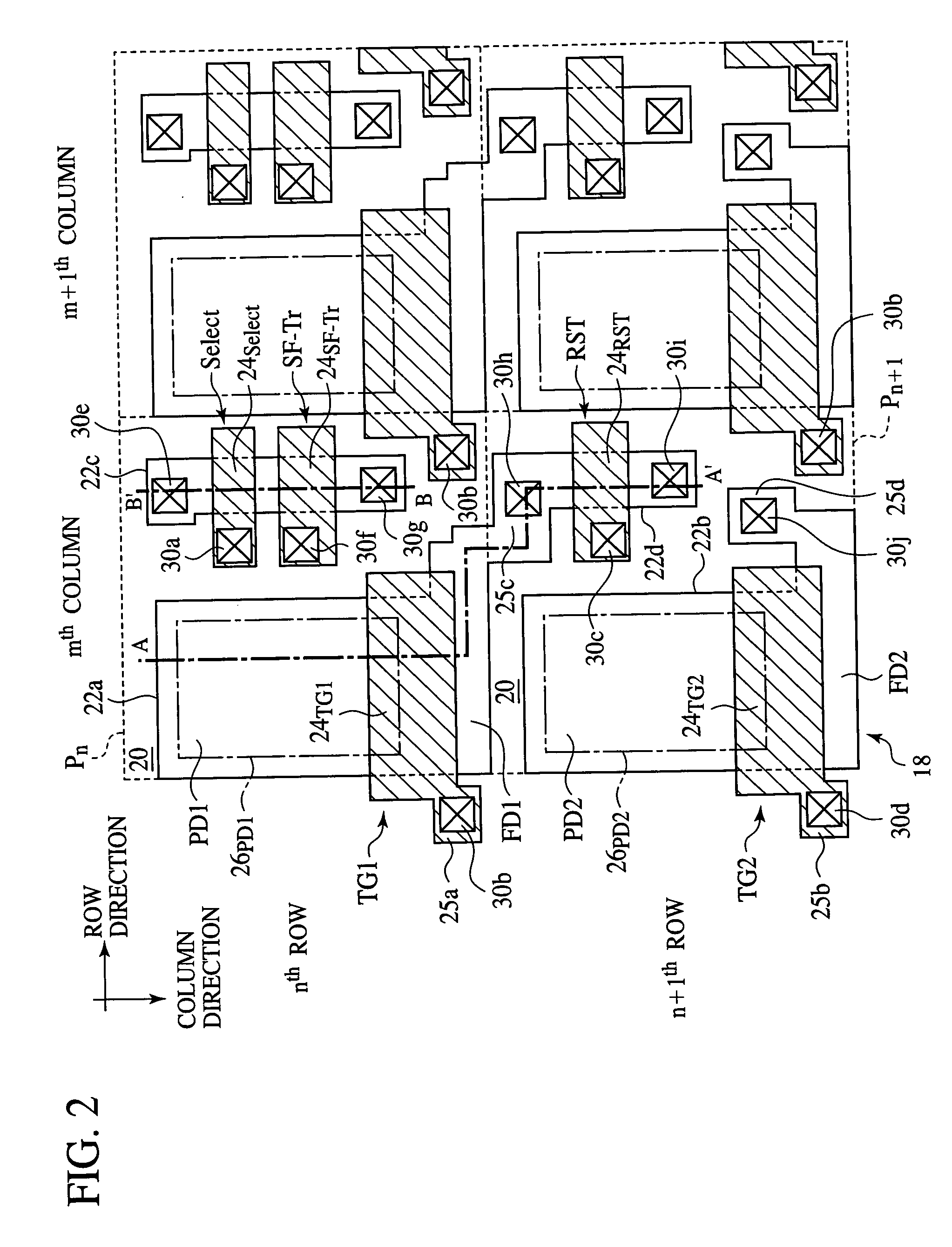
[0054] The solid-state image sensor according to a first embodiment of the present invention will be explained with reference to FIGS. 1 to 10. FIG. 1 is a circuit diagram of the solid-state image sensor according to the present embodiment. FIGS. 2 to 5 are plan views of the solid-state image sensor according to the present embodiment, which show a structure thereof. FIGS. 6A-6B to 10 are sectional views of the solid-state image sensor according to the present embodiment in the steps of the method for fabricating the same, which show the method.

[0055] First, the structure of the solid-state image sensor according to the present embodiment will be explained with reference to FIGS. 1 to 5.

[0056] The solid-state image sensor according to the present embodiment is a solid-state image sensor including 4-Tr-pixels having elements made common between the pixels. That is, in the solid-state image sensor according to the present embodiment, a plurality of pixels each incl...

second embodiment

A Second Embodiment

[0168] The solid-state image sensor according to a second embodiment of the present invention will be explained with reference to FIGS. 11 to 16. FIGS. 11 to 13 are plan view of the solid-state image sensor according to the present embodiment, which show a structure thereof. FIGS. 14 to 16 are sectional view of the solid-state image sensor according to the present embodiment in the steps of the method for fabricating the same, which show the method. The same members of the present embodiment as those of the solid-state image sensor according to the first embodiment are represented by the same reference numbers not to repeat or to simplify their explanation.

[0169] The solid-state image sensor according to the present embodiment is the same in the circuit diagram, the basic structure and the fabrication method as the solid-state image sensor according to the first embodiment except that the first and the second metal interconnection layers 32, 26 are different from...

third embodiment

A Third Embodiment

[0206] Next, the solid-state image sensor according to a third embodiment of the present invention will be explained with reference to FIG. 18. FIG. 18 is a plan view of the solid-state image sensor according to the present embodiment, which shows a structure thereof. The same members of the present embodiment as those of the solid-state image sensor according to the first embodiment are represented by the same reference numbers not to repeat or to simplify their explanation.

[0207] The solid-state image sensor according to the present embodiment is the same in the circuit diagram, the basic structure and the fabrication method as the solid-state image sensor according to the first embodiment except that the plane shape of the gate electrodes 24TG1, 24TG2 of the transfer transistors TG1, TG2 are different. The structure of the solid-state image sensor according to the present embodiment will be explained with reference to FIG. 18. FIG. 18 is a plan view of the layo...


PUM


Abstract

In the solid-state image sensor including 4-Tr-pixels, a source follower transistor SF-Tr, a rest transistor RST and a select transistor Select are made common between pixels Pn, Pn+1 adjacent in the column direction, and a transfer transistor TG1 and a transfer transistor TG2 are formed in region which respectively positioned on the same side with respect to the photodiode PD1 and the photodiode PD2, and the source follower transistor SF-Tr, the reset transistor RST and the select transistor Select made common are formed in regions positioned on the side in the row direction with respect to the photodiode PD1 and the photodiode PD2.

Description

CROSS-REFERENCE TO RELATED APPLICATIONS [0001] This application is based upon and claims priority of Japanese Patent Application No. 2004-130806, filed on Apr. 27, 2004, the contents being incorporated herein by reference. BACKGROUND OF THE INVENTION [0002] The present invention relates to a solid-state image sensor including common elements between the pixels. [0003] The solid-state imaging device using semiconductors are roughly classified in CCDs and image sensors based on CMOS. [0004] The CMOS image sensors generally have the structure which is the so-called 3-Tr APS (Active Pixel Sensor), comprising a photodiode (PD) which converts a photo signal to an electric signal, a reset transistor (RST) which resets the photodiode, a source follower transistor (SF-Tr) which converts signal charges of the photodiode to voltages to output the signal charges in voltage, and a select transistor (Select) which connects / selects pixels and signal lines. [0005] It is said that the solid-state im...

Claims


Application Information

Patent Timeline
Patent Type & Authority Applications(United States)
IPC IPC(8): H01L27/146H01L31/10H04N5/335H04N5/357H04N5/369H04N5/374
CPCH01L27/14641H01L27/14609H01L27/146H04N25/77
Inventor OHKAWA, NARUMI
Owner FUJITSU SEMICON LTD
Why Eureka
Try Eureka