Data output apparatus for memory device

a data output and memory device technology, applied in the direction of digital storage, instruments, other accessories, etc., can solve the problems of inability to use the conventional apparatus for the next generation memory device, difficult to reduce the delay time, etc., to reduce the delay elements of data transferring, improve the speed of data transferring, and reduce the read operation time of the memory device

Inactive Publication Date: 2005-10-27
INTELLECTUAL DISCOVERY CO LTD
View PDF9 Cites 2 Cited by
  • Summary
  • Abstract
  • Description
  • Claims
  • Application Information

AI Technical Summary

Benefits of technology

[0027] Another object of the present invention is to provide a data output apparatus capable of reducing a read operation time of a memory device by improving a speed of data transferring through reducing delay elements of data transferring.

Problems solved by technology

However, the conventional apparatus has many delay elements (the inverters INV3, INV4 and the switches TM1 and TM2), so it is difficult to reduce the delay time.
Thus, it is not available to use the conventional apparatus for the next generation memory device which operates speedy such as DDR2 SDRAM.

Method used


Image

  • Data output apparatus for memory device
  • Data output apparatus for memory device
  • Data output apparatus for memory device

Examples


Embodiment Construction

[0034] Reference will now be made in greater detail to a preferred embodiment of the invention, an example of which is illustrated in the accompanying drawings. Wherever possible, the same reference numerals will be used throughout the drawings and the description to refer to the same or like parts.

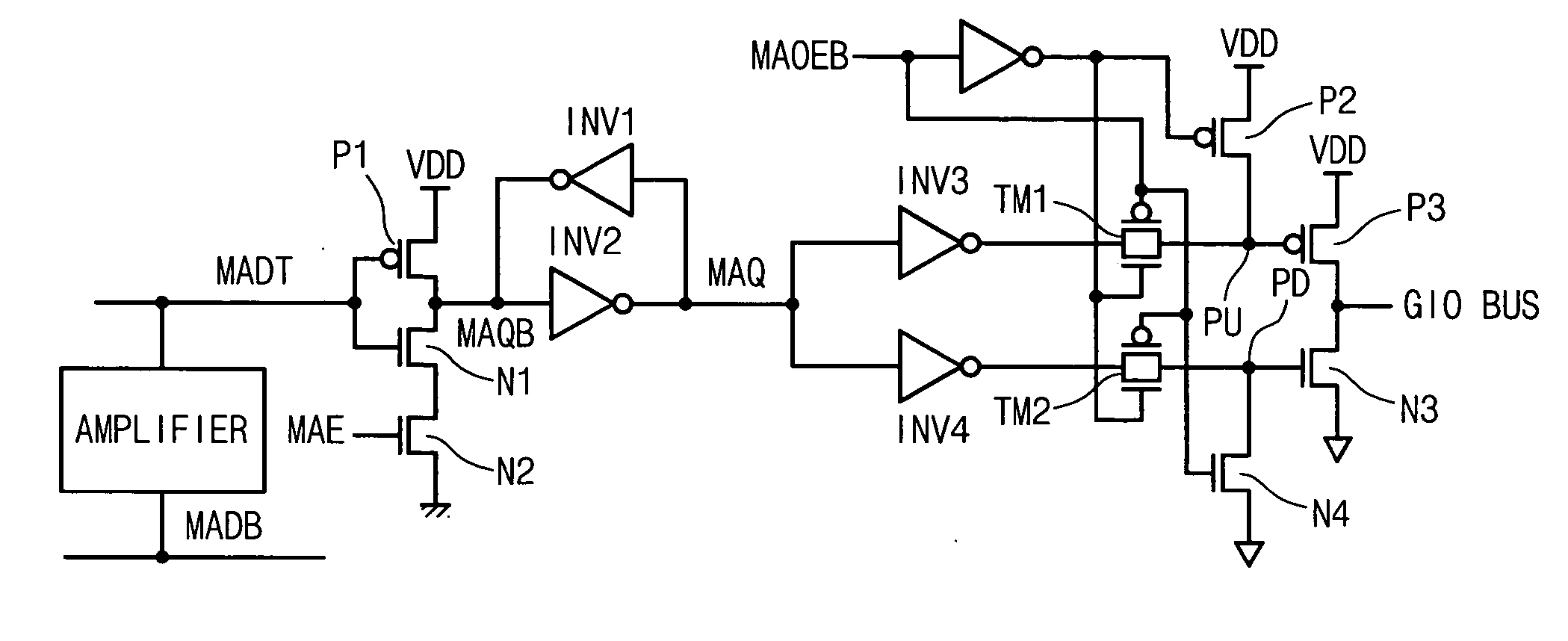
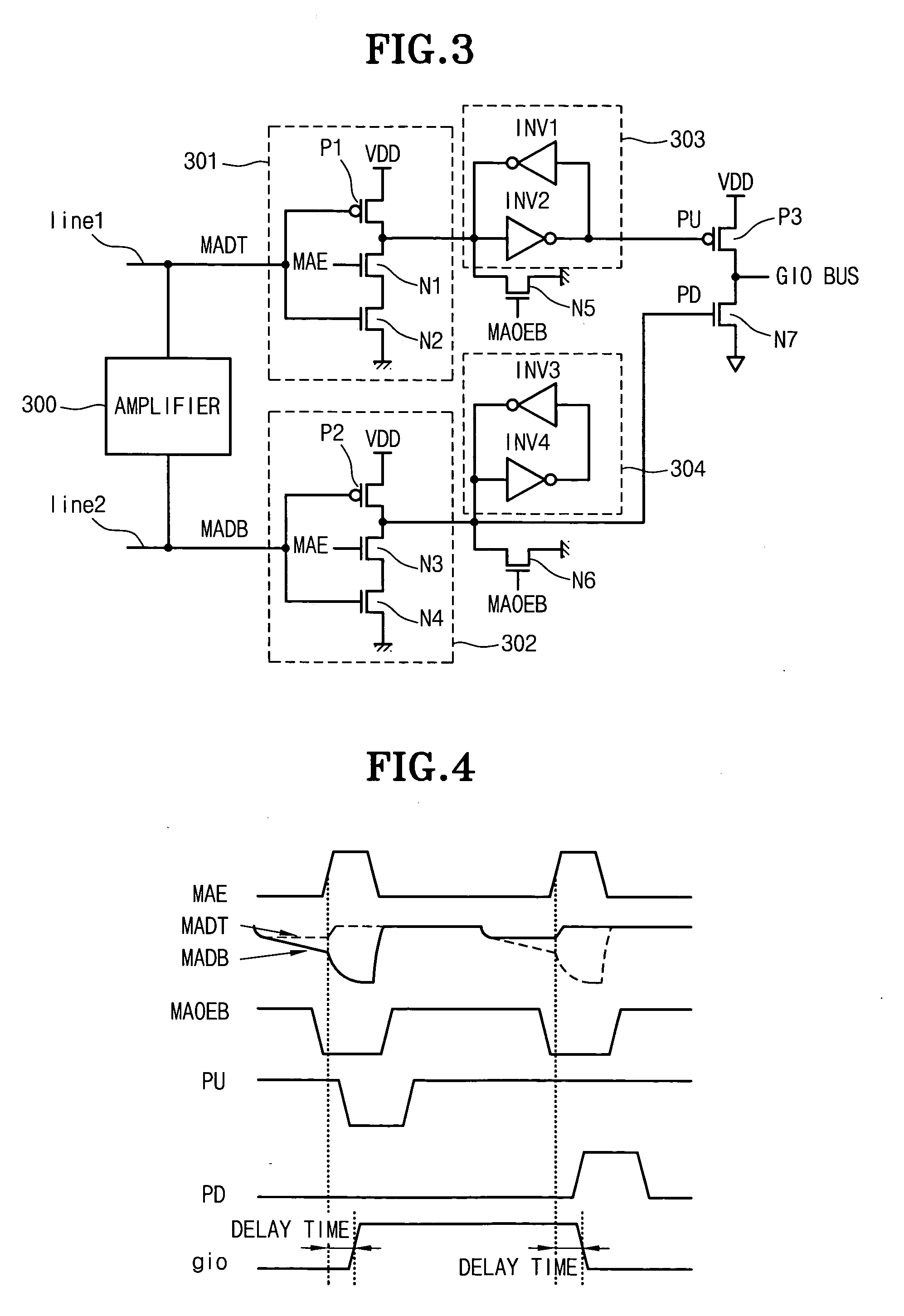
[0035]FIG. 3 is a circuit diagram illustrating an exemplary embodiment a data output apparatus for a memory device in accordance with the present invention.

[0036] The data output apparatus for the memory device is comprised of local data lines line1, line2, an amplifier 300, CMOS buffers 301, 302, latches 303, 304, and the pull-up transistor P13 and the pull-down transistor N17.

[0037] The local data lines line1, line2 receive data transferred from a pair of bitlines BIT, / BIT of the memory device. As shown in FIG. 3, a MADT is a data on the local data line line1, a MADB is another data on the local data line line2. As described above, it's merely about 200 mV, as aforementioned, for a ...


PUM


Abstract

The present invention relates to a data output apparatus for a memory device, and more particularly to, a data output apparatus improved a data transferring speed by re-amplifying a data amplified by a bitline sense amplifier and transferring it to global input/output lines. The data output apparatus comprises: first and second local data lines for receiving data transferred from a pair of bitlines of a memory device; an amplifier interposed between the first and second local data lines; a first CMOS buffer means for receiving data on the first local data line; a second CMOS buffer means for receiving data on the second local data line; a first latch means for holding an output signal of the first CMOS buffer means; a second latch means for holding an output signal of the second CMOS buffer means; and a pull-up transistor and a pull-down transistor coupled between a driving voltage and a ground terminal in series. Here, an output signal of the first latch means is applied to a gate of the pull-up transistor, while an output signal of the second latch means is applied to the pull-down transistor.

Description

BACKGROUND OF THE INVENTION [0001] 1. Field of the Invention [0002] The present invention relates to a data output apparatus in a memory device, and more particularly to, a data output apparatus improved a data transferring speed by re-amplifying a data amplified by a bitline sense amplifier and transferring it to global input / output lines [0003] 2. Description of the Related Art [0004] In general, during a read operation of a memory device, a cell data selected by an address signal is transferred to a local data line after being sensed and amplified by a bitline sense amplifier. Typically, a bitline and a local data line are comprised of a pair, respectively. [0005] However, it is merely about 20 mV for the differences between high level and low level of the data transferred to the local data lines. As a result, it is necessary to perform processes for converting the data to a CMOS voltage level. Those processes are performed by an amplifier(with reference to an amplifier in FIG. 1...

Claims


Application Information

Patent Timeline
Patent Type & Authority Applications(United States)
IPC IPC(8): G11C5/00G11C7/10
CPCG11C7/1051G11C7/1087G11C7/1069A45C11/00A45C2011/002
Inventor KIM, DONG KYUN
Owner INTELLECTUAL DISCOVERY CO LTD
Why Eureka
Try Eureka