Flexible 2T-based fuzzy and certain matching arrays

a two-transistor, nvm cell technology, applied in static storage, digital storage, instruments, etc., can solve the problems of inability to provide in-circuit real-time programmability, increase the hassle of erase time, increase the design challenge, etc., to achieve better scalability during program operation and reduce noise during read operation

Inactive Publication Date: 2014-12-23
APLUS FLASH TECH
View PDF14 Cites 2 Cited by
  • Summary
  • Abstract
  • Description
  • Claims
  • Application Information

AI Technical Summary

Benefits of technology

[0024]The seventh object of this invention is to identify and select a high-voltage Flash transistor for implementing above said one paired 2T NVM cell. The 2T Flash cell array and cell's Vt assignment are made to be the same as above third objective except the SL layout in array is made to run in Y-axis in parallel to all BL for noise reduction during read operation and better scalability during program operation. Unlike traditional array, many vertical BLs share one common SL running in X-axis, each single BL has one dedicate SL in parallel.

Problems solved by technology

The disadvantage of the ROM-based PLD is that it cannot provide an in-circuit real time programmability.
Any one of negative value of Vt0 or Vt1 would result in the BL leakage, thus malfunction of PLD operation.
Another disadvantage of this prior 1T PLD NOR-array is the encountering of the over-erase issue that would increase the hassle of erase time and the design challenge.

Method used


Image

  • Flexible 2T-based fuzzy and certain matching arrays
  • Flexible 2T-based fuzzy and certain matching arrays
  • Flexible 2T-based fuzzy and certain matching arrays

Examples


Embodiment Construction

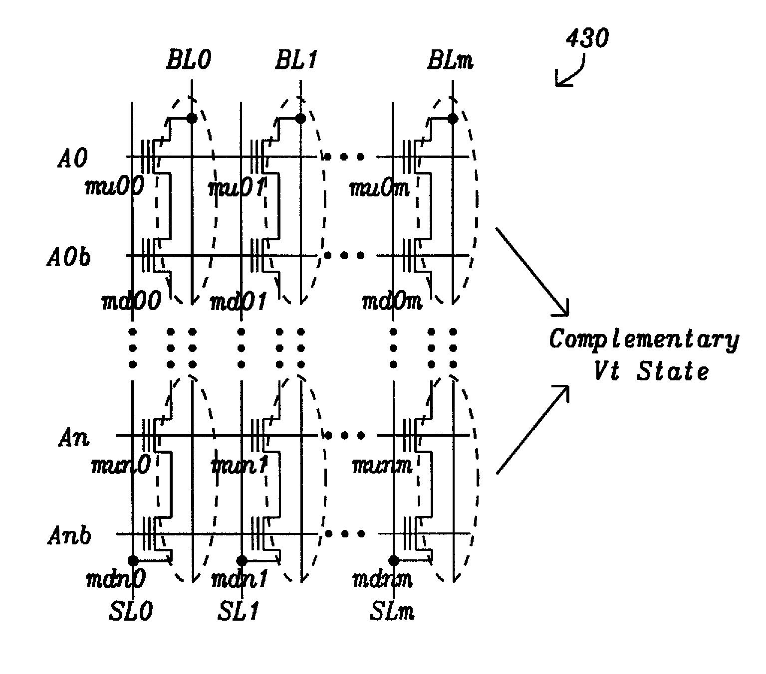
[0052]Unlike prior art, each PLD, PAL or Comparison cell of the present invention is connected in series as an unit cell to configure it into a NAND-array. The two gates of each 2T-cell are connected to two wordlines (WLs), which are connected to two complementary logic inputs. The two threshold voltages (Vts) of 2T non-volatile memory (NVM) transistors are also made complementary for the accurate PLD, PAL and Comparison implementation. For n-bit logic inputs, then the total number of WLs would be 2n which is due to the n paired 2T cells' gates number plus one common BL (Biltine).

[0053]Similarly, another embodiment of the present invention is to extend the 2T-cell NAND-array to 2nT-cell NAND array for n-bit PAL, PLD and matching and comparison functions, comprises of 2n Flash transistors that are also connected in series as a n-bit unit storage cell. The preferable NVM transistors of 2T cell or 2nT cell of the present invention are using the traditional LV (low-voltage) ROM or HV (h...


PUM


Abstract

A novel NVM-based 2T or 2nT NAND-cell for a NAND-array for PLD, PAL and matching functions is disclosed. The preferable NVM cell can be ROM or Flash. The 2T flash cell preferably uses FN for both program and erase operation, while 2T ROM cell preferably to use phosphorus for ROM code implant to get negative Vt0.

Description

[0001]This application claims priority to U.S. Provisional Patent Application Ser. No. 61 / 461,044, filed Jan. 11, 2011, which is owned by a common assignee, and which is herein incorporated by reference in its entirety.RELATED APPLICATION[0002]This application is related to the following US patent application issued as U.S. Pat. No. 8,072,811, issued Dec. 6, 2011, titled “NAND based NMOS NOR flash memory cell, a NAND based NMOS NOR flash memory array, and a method of forming a NAND based NMOS NOR flash memory array”, application Ser. No. 12 / 387,771, which is incorporated by reference in their entirety and is assigned to a common assignee as the instant application.BACKGROUND OF INVENTION[0003](1) Field of the Invention[0004]This invention relates generally to a novel two-transistor (2T) based NVM cell array that is most suitable for traditional Programmable Logic Device (PLD), Programmable Array Logic (PAL) and any matching and comparing function applications.[0005](2) Description o...

Claims


Application Information

Patent Timeline
Patent Type & Authority Patents(United States)
IPC IPC(8): G11C11/34G11C16/10G11C16/04
CPCG11C16/0483G11C16/10G11C16/0441
Inventor LEE, PETER WUNGHSU, FU-CHANG
Owner APLUS FLASH TECH
Why Eureka
Try Eureka