Method of synthesizing colloidal nanocrystals

a colloidal nanocrystal and nanocrystal technology, applied in the field of semiconductor nanocrystal synthesis, can solve the problems of difficult control of the quality of such nanocrystals, high cost, explosive, etc., and achieve the effect of low cos

Active Publication Date: 2005-10-27
NAT RES COUNCIL OF CANADA
View PDF3 Cites 18 Cited by
  • Summary
  • Abstract
  • Description
  • Claims
  • Application Information

AI Technical Summary

Benefits of technology

[0019] The novel synthetic approaches adopted in the present invention do not involve the use of acids, and thus are completely different from those reported and used elsewhere at present. The synthetic route is shorter and the costs are lower. In addition, with the synthetic scheme proposed here, it is easy to prepare “high quality” CdSe nanoparticles of various sizes, especially “large” ones with yellow to red emission colours (580 nm-650 nm) wavelength.

Problems solved by technology

However, it has generally been found difficult to control the quality of such nanocrystals.
Cd(CH3)2 is toxic, pyrophoric, expensive, unstable at room temperature in air, and explosive due to the release of gas during synthesis.
This organometallic approach requires extremely restrictive synthetic equipment and conditions.
However, this method requires the use tri-n-octylphospine oxide and an acid.
However, it has been acknowledged that the demonstration of PL intensity by the QY is problematic, primarily because of the significant difference in QY values when different dyes are used.

Method used


Image

  • Method of synthesizing colloidal nanocrystals
  • Method of synthesizing colloidal nanocrystals
  • Method of synthesizing colloidal nanocrystals

Examples


example 1

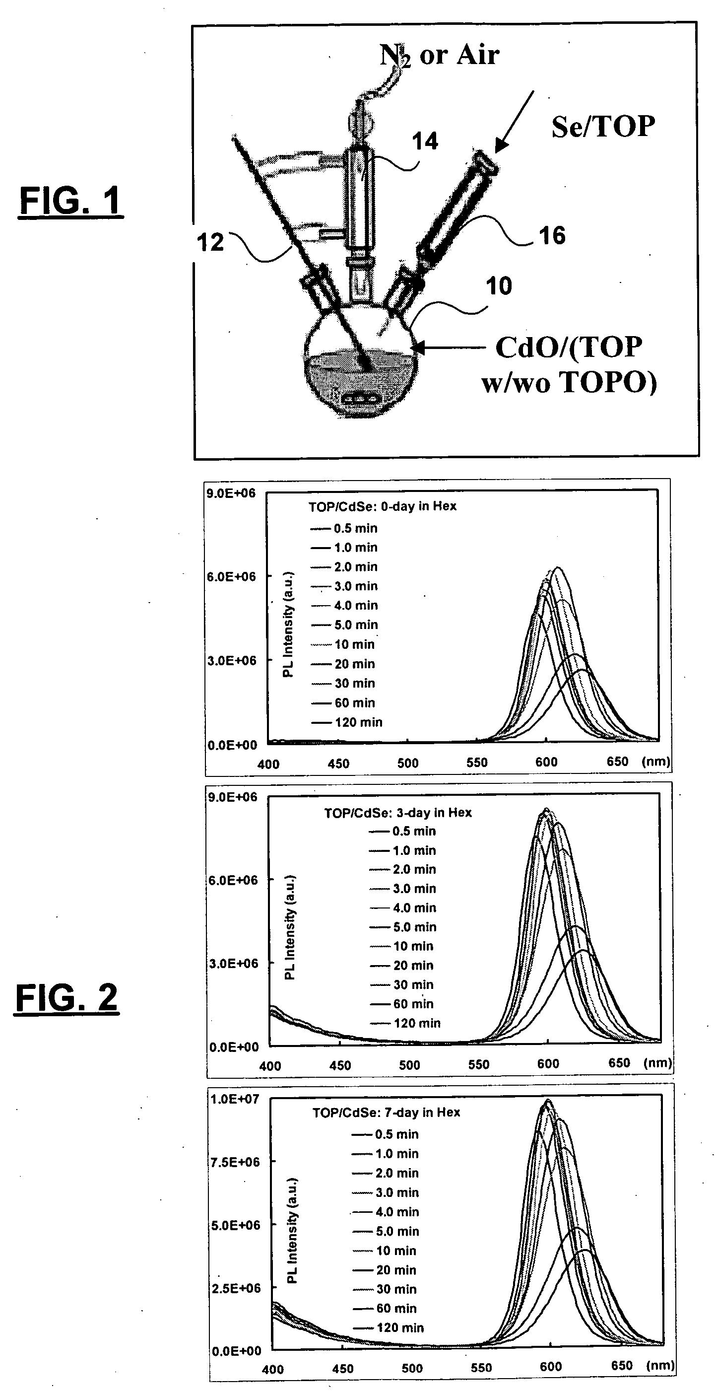
[0074] TOP-capped CdSe was made by adding a solution of TOP / Se to CdO in TOP under the following conditions: [0075] CdO=12.8 mg (0.10 mmol) [0076] Se=3.78 mg (0.05 mmol) [0077] Cd / Se=2:1 [0078] TOP=1.58 g [0079] CdO=63.3 mmol / kg [0080] Nucleation temperature=300° C. [0081] growth temperature =250 C

[0082]FIG. 2 shows the PL spectra of CdSe with one-component surface ligands (namely TOP), dispersed in Hex, after 0 day (up), 3 days (middle), and 7 days (down).

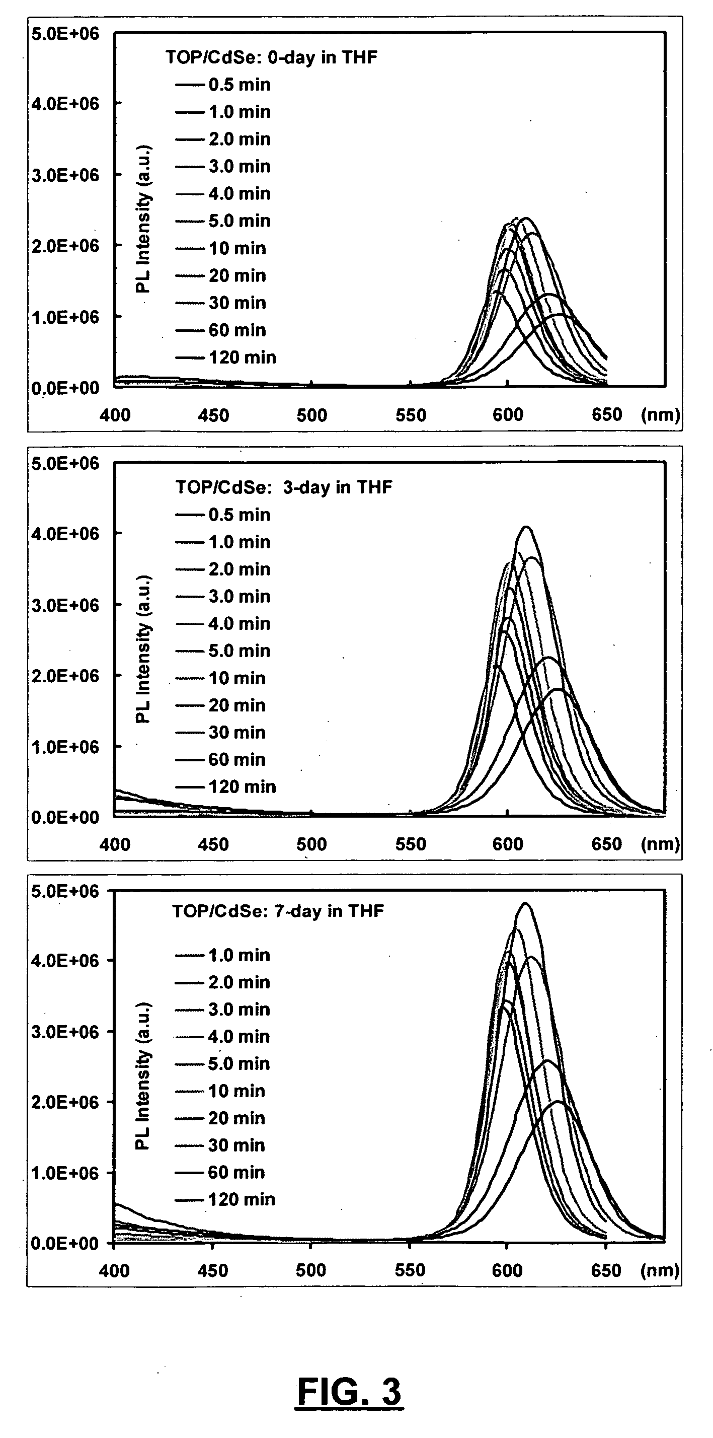
[0083]FIG. 3 show the PL spectra of as-synthesized CdSe with one-component surface ligands (namely TOP), dispersed in THF, after 0 day (up), 3 days (middle), and 7 days (down).

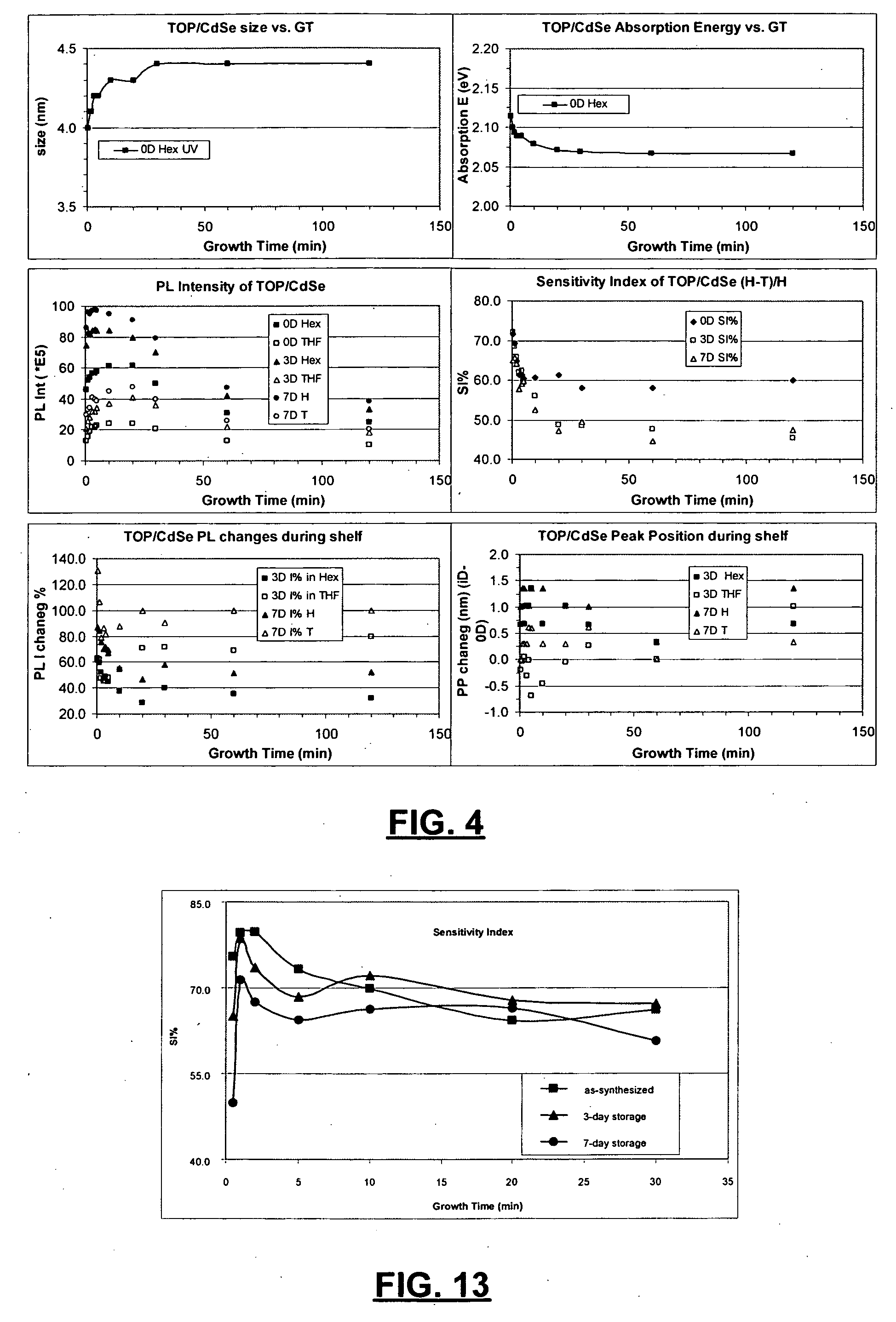
[0084]FIG. 4 is an analysis of the UV and PL characterization of the as-synthesized CdSe with one-component surface ligands, dispersed in Hex and THF. The shelf time in Hex or THF is 3 days and 7 days.

[0085]FIG. 5 shows the PL spectra of CdSe with one-component surface ligands (TOP) dispersed in various solvents, the nanocrystals were two-day old after s...

example 2

[0088] CdSe was made by adding a solution of TOP / Se to Cd(Ac)2 in TOP under the following conditions: [0089] Cd(Ac)2=23.08 mg (0.10 mmol) [0090] Se=3.95 mg (0.05 mmol) [0091] Cd / Se=2:1 [0092] TOP=2.814 g; [0093] Cd(Ac)2=35.7 mmol / kg [0094] Nucleation temperature=300° C. [0095] growth temperature=250° C.

[0096]FIG. 8 shows the PL spectra of the synthesized CdSe with one-component surface ligands (namely TOP), dispersed in Hex (up) and THF (down).

example 3

[0097] TOP-capped CdTe as made under the following conditions: [0098] CdO=12.85 mg (0.10 mmol) [0099] Te=5.70 mg (0.05 mmol) [0100] Cd / Te=2:1 [0101] TOP=1.56 g [0102] CdO=64 mmol / kg [0103] Nucleation temperature=300° C. [0104] growth temperature=250° C.

[0105]FIG. 9 shows the PL spectra of as-synthesized CdTe with one-component surface ligands (namely TOP), dispersed in Hex. The PL intensity vs. growth time is plotted and inserted.


PUM

PropertyMeasurementUnit
temperatureaaaaaaaaaa
molar ratioaaaaaaaaaa

Abstract

A method of making nanocrystals involves adding a chalocogen source to a hot solution of a metal-containing non-organometallic compound, such as CdO, in a first ligand solvent, such as TOP, and preferably subsequently cooling the resulting mixture to a lower temperature to grow the nanocrystals at said lower temperature. The method can involve either one ligand or two-ligand systems.

Description

CROSS REFERENCE TO RELATED APPLICATIONS [0001] This application claims the benefit under 35 USC 119(e) of prior U.S. application No. 60 / 533,887 filed Dec. 30, 2003 and 60 / 544,325 filed Feb. 17, 2004, the contents of which are herein incorporated by reference.FIELD OF THE INVENTION [0002] The present invention relates to the field of semi-conductor nanocrystal technology, and in particular to the synthesis of semi-conductor nanocrystals. These nanocrystals can be used for various applications, such as labelling and sensing. BACKGROUND OF THE INVENTION [0003] Semiconductor nanocrystals are nanoparticles composed of an inorganic, crystalline semiconductive material and have unique photophysical, photochemical and nonlinear optical properties arising from quantum size effects, and have therefore attracted a great deal of attention for their potential applicability in a variety of contexts, e.g., as detectable labels in biological applications, and as useful materials in the areas of pho...

Claims


Application Information

Patent Timeline
Patent Type & Authority Applications(United States)
IPC IPC(8): C01B13/32C01B17/20C01B19/00C01B25/14C01G1/00C01G1/12C01G11/00C30B7/08C30B29/46
CPCB82Y30/00Y10S977/825C01B17/20C01B19/007C01G1/00C01G1/12C01G11/00C01P2002/72C01P2002/84C01P2002/86C01P2004/64Y10S977/773Y10S977/775Y10S977/774Y10S977/824Y10S977/813C01B13/328
Inventor YU, KUIRIPMEESTER, JOHN
Owner NAT RES COUNCIL OF CANADA
Why Eureka
Try Eureka