Bonding structure for flat panel display, method of forming the same, and flat panel display including bonding structure

a flat panel display and bonding structure technology, applied in the field of flat panel displays, can solve the problems of reducing the image quality of the panel, lcos panel having small pixels, image damage, etc., and achieve the effect of preventing an infiltration of a sealant into an active area and constant cell gap

Active Publication Date: 2005-10-27
SAMSUNG ELECTRONICS CO LTD
View PDF11 Cites 24 Cited by
  • Summary
  • Abstract
  • Description
  • Claims
  • Application Information

AI Technical Summary

Benefits of technology

[0010] The present invention provides a bonding structure of a flat panel display device, wh...

Problems solved by technology

However, in a case where the LCOS panel having a fine cell gap is manufactured with respect to the response time of the liquid crystal, an optical interference may occur due to different sizes of cell gaps on the panel, thereby causing a reduction in the image quality of the panel.
The above problem is caused by the different thermal properties of an upper substrate and a lower substrate in bonding the upper and lower substrates, or the fine cell gap.
However, the above methods cause problems in the LCOS panel having small pixels, unlike the LCD.
That is, in a case where the spacer is applie...

Method used


Image

  • Bonding structure for flat panel display, method of forming the same, and flat panel display including bonding structure
  • Bonding structure for flat panel display, method of forming the same, and flat panel display including bonding structure
  • Bonding structure for flat panel display, method of forming the same, and flat panel display including bonding structure

Examples


Embodiment Construction

[0024] Hereinafter, a bonding structure of a flat panel display, a method of forming the bonding structure, and a flat panel display having the bonding structure according to exemplary embodiments of the present invention will be described with reference to accompanying drawings.

[0025] A bonding structure of a flat panel display according to the present invention will be described as follows.

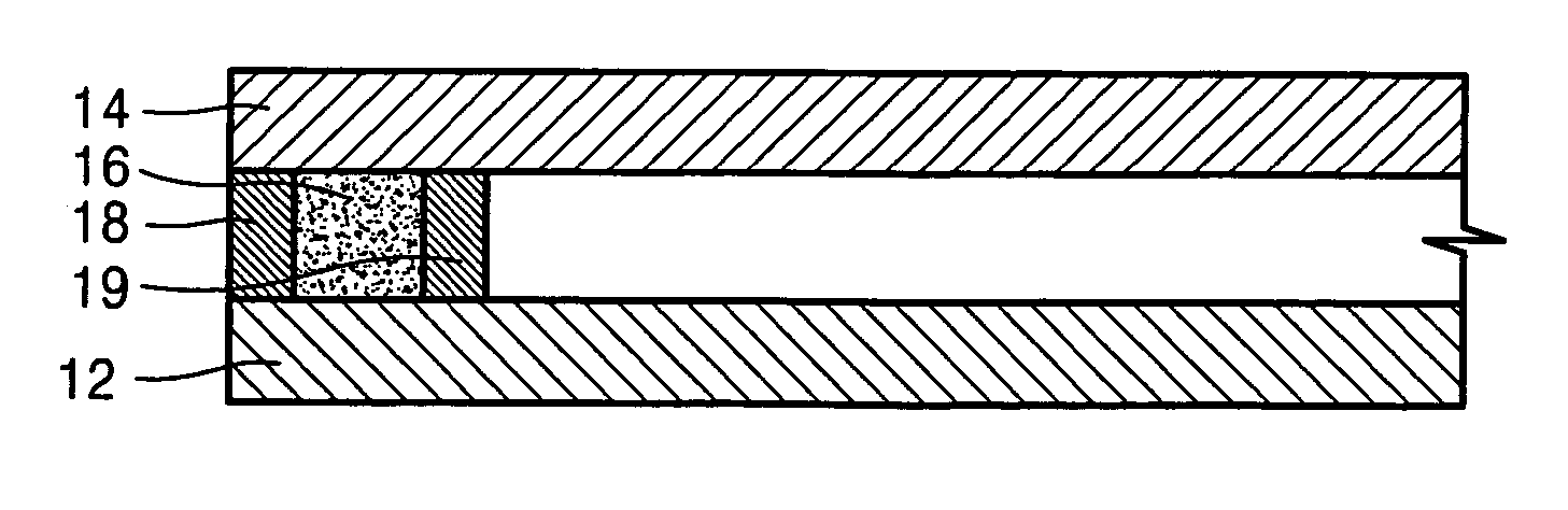
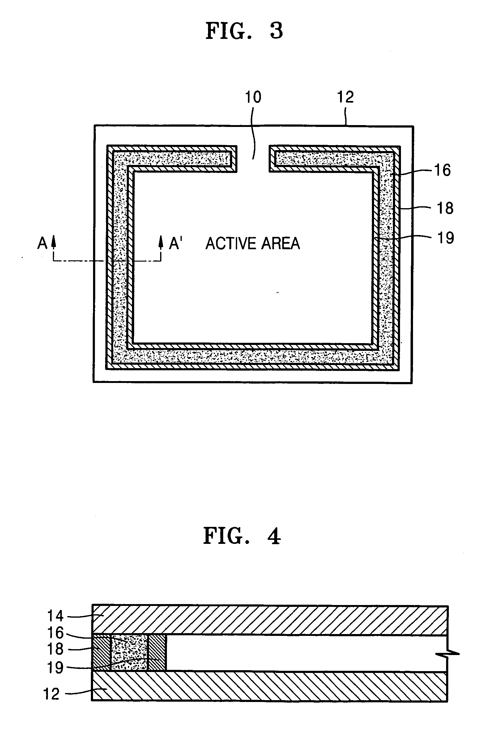
[0026]FIG. 3 is a plane view of a flat panel display showing an arranging form of the bonding structure according to an exemplary embodiment of the present invention, and FIG. 4 is a cross-sectional view taken along line A-A′ of FIG. 3.

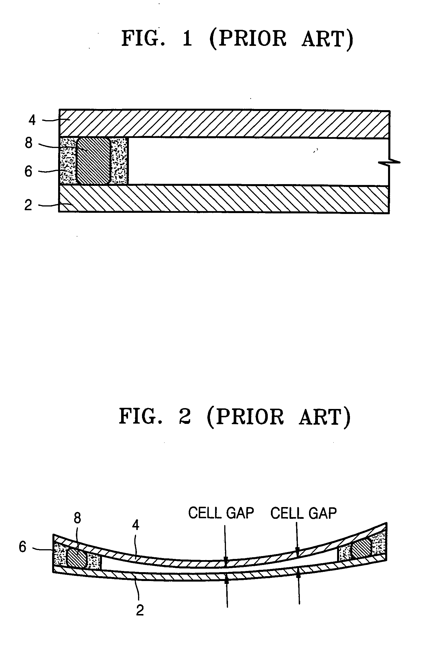
[0027] Referring to FIGS. 3 and 4, the bonding structure of the flat panel display is formed between an upper substrate 14 and a lower substrate 12 of the flat panel display to seal and bond the two substrates 12 and 14 to each other. The bonding structure includes an outer separation wall 18 and an inner separation wall 19, which are of equal heights and dispo...


PUM

PropertyMeasurementUnit
Widthaaaaaaaaaa
Widthaaaaaaaaaa
Heightaaaaaaaaaa

Abstract

Provided are a bonding structure for a flat panel display and a method of forming the same, and a flat panel display, including the bonding structure. The bonding structure of a flat panel display device, which is formed between an upper substrate and a lower substrate to seal and bond the two substrates of the flat panel display device, and the bonding structure includes an outer separation wall and an inner separation wall of same heights being arranged along edges of the upper substrate and the lower substrate with a predetermined interval, and a sealant being applied between the outer separation wall and tn wall.

Description

BACKGROUND OF THE INVENTION [0001] Priority is claimed to Korean Patent Application No. 2004-28162, filed on Apr. 23, 2004, in the Korean Intellectual Property Office, the disclosure of which is incorporated herein in its entirety by reference. [0002] 1. Field of the Invention [0003] The present invention relates to a flat panel display, and more particularly, to a bonding structure for sealing and bonding an upper substrate and a lower substrate of a flat panel display, a method of forming the bonding structure, and a flat panel display having the bonding structure. [0004] 2. Description of the Related Art [0005] A flat panel display can be classified as: a liquid crystal display (LCD), a plasma display panel (PDP), or a field emission display (FED). Recently, a liquid crystal on silicon (LCOS), which forms a thin film transistor (TFT) on a silicon substrate and uses a liquid crystal to display an image, is highlighted due to the demand for a micro-display. [0006] The LCOS panel is...

Claims


Application Information

Patent Timeline
IPC IPC(8): G02F1/1341G02F1/1333G02F1/1339G09F9/30H01J9/24H01J9/26H01J9/39
CPCG02F1/1339H01J9/242Y10T428/24777H01J9/39H01J9/261G02F1/1341
Inventor KIM, SU-GUNPARK, SANG-MOOHYUN, SOON-YOUNGKIM, WON-NYUNWANG, JONG-MINLEE, GYU-MIN
Owner SAMSUNG ELECTRONICS CO LTD
Why Eureka
Try Eureka