Method for manufacturing a complementary metal-oxide semiconductor sensor

Active Publication Date: 2005-11-03
UNITED MICROELECTRONICS CORP
View PDF3 Cites 0 Cited by
  • Summary
  • Abstract
  • Description
  • Claims
  • Application Information

AI Technical Summary

Benefits of technology

[0013] Accordingly, it is one objective of the present invention to provide a method for manufacturing complementary metal-oxide semiconductor sensors. The present invention coats a sacrificial layer formed on a protective layer of a CMOS sensor to prevent particles from dropping.
[0014] It is another objective of the present invention to provide a method for manufacturing complementary metal-oxide semiconductor sensors. The present invention provides a sacrificial layer formed on a protective layer to prevent the CMOS sensor from broken due to particles to increase the yield for manufacturing the CMOS sensors.
[0015] It is a further objective of the present invention to provide a method for manufacturing complementary metal-oxide semiconductor sensors. The present invention provides a sacrificial layer formed on a protective layer to increase the preventive maintenance period for manufacturing the CMOS sensors.
[0016] It is a further objective of the present

Problems solved by technology

The yield for manufacturing the MOS sensors is reduced due to the broken MOS sensors.
Even if the bell jar 112 having a rougher surface does adhere little more particles 106′, the improvement due to the ceramic layer is still not g

Method used


Image

  • Method for manufacturing a complementary metal-oxide semiconductor sensor
  • Method for manufacturing a complementary metal-oxide semiconductor sensor
  • Method for manufacturing a complementary metal-oxide semiconductor sensor

Examples


Example

[0021] These preferred embodiments of the present invention are now described in greater detail. Nevertheless, it should be recognized that the present invention can be practiced in a wide range of other embodiments besides those explicitly described, and the scope of the present invention is expressly not limited except as specified in the accompanying claims.

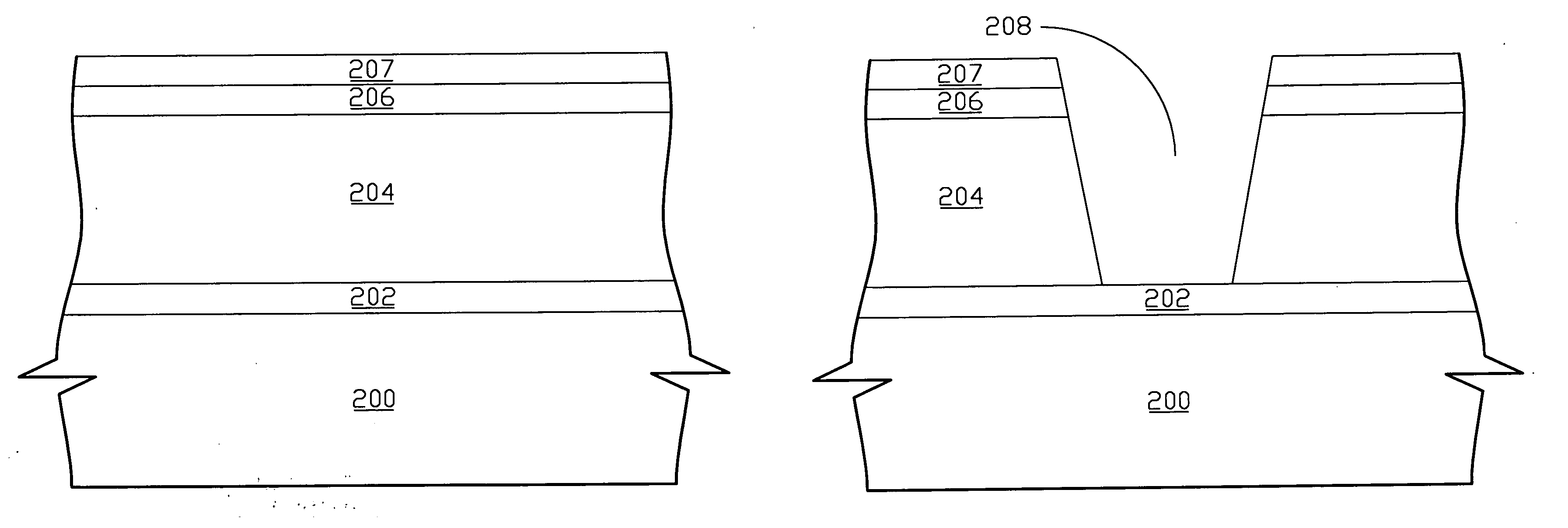
[0022] As illustrated in FIG. 2A, the embodiment of the present invention provides a semiconductor structure 200 including elements of a CMOS sensor, wherein the whole CMOS sensor and the elements of the CMOS sensor are not shown in FIG. 2A. A plurality of conductors 202 is applied on the semiconductor structure 200, wherein there is only a conductor 202 shown in FIG. 2A. A dielectric layer, i.e. an IMD layer 204, is formed, e.g. deposited, onto the conductors 202. The IMD layer 204 may cover portions of the semiconductor structure 200 that are not covered by conductors 202. A protective layer, i.e. a silicon nitride film 206...


PUM


Abstract

A method for manufacturing a complementary metal-oxide semiconductor sensor is provided. The present method provides a semiconductor structure including a plurality of conductors thereon. An inter-metal dielectric layer is formed on the conductors. A silicon nitride film is applied on the inter-metal dielectric layer. An oxide layer is formed on the silicon nitride film. The oxide layer, the silicon nitride film and the inter-metal dielectric are etched to expose portions of the conductors. The oxide layer and the exposed conductors are cleaned in a cleaning step later.

Description

BACKGROUND OF THE INVENTION [0001] 1. Field of the Invention [0002] The present invention relates to a method for manufacturing a metal-oxide semiconductor sensor, and more particularly to a method for manufacturing a metal-oxide semiconductor sensor having a more oxide layer. [0003] 2. Description of the Prior Art [0004] For manufacturing a metal-oxide semiconductor sensor, a protective layer for preventing the inter-metal dielectric layer, IMD layer, from plasma damage to reduce dark current is formed on the inter-metal dielectric layer. [0005] As shown in FIG. 1A, a semiconductor structure 100 including elements, e.g. a source, a gate, a drain, etc., of a MOS sensor is provided, wherein the elements of the MOS are not shown in FIG. 1A. A plurality of conductors 102 is applied on the semiconductor structure 100, wherein there is only a conductor 102 shown in FIG. 1A. An inter-metal dielectric layer 104, IMD layer, is deposited onto the conductors 102. The IMD layer 104 may cover p...

Claims


Application Information

Patent Timeline
IPC IPC(8): C23C16/00H01L21/02H01L21/336H01L21/768H01L21/8234
CPCH01L21/76814H01L21/02063
Inventor LIN, CHI-RONGJIANG, NIEN-CHUNGCHANG, CHIH-SHENG
Owner UNITED MICROELECTRONICS CORP
Why Eureka
Try Eureka