

Atomic implantation and thermal treatment of a semiconductor layer
a technology of atomic implantation and thermal treatment, which is applied in the direction of semiconductor/solid-state device manufacturing, basic electric elements, electric devices, etc., can solve the problems of satisfactory solution, delamination at the edge of the bonding layer, and the least partial detachment of the bonding interface, so as to achieve the effect of reducing surface roughness
- Summary
- Abstract
- Description
- Claims
- Application Information
AI Technical Summary
Benefits of technology
Problems solved by technology
Method used
Image

Examples
Embodiment Construction
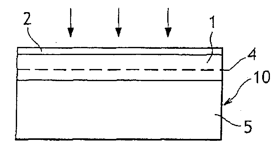
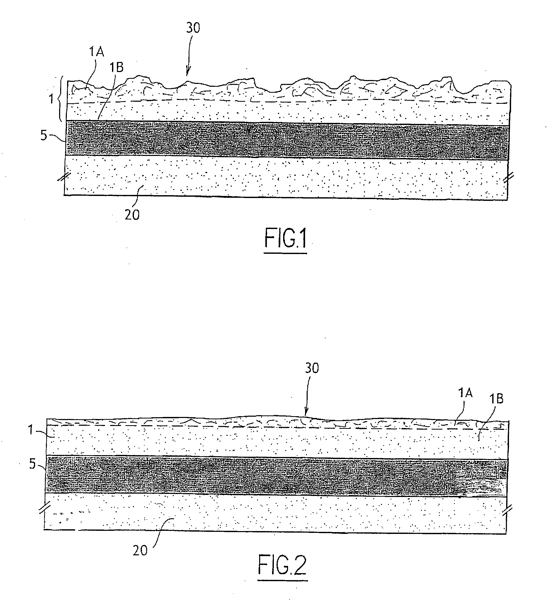
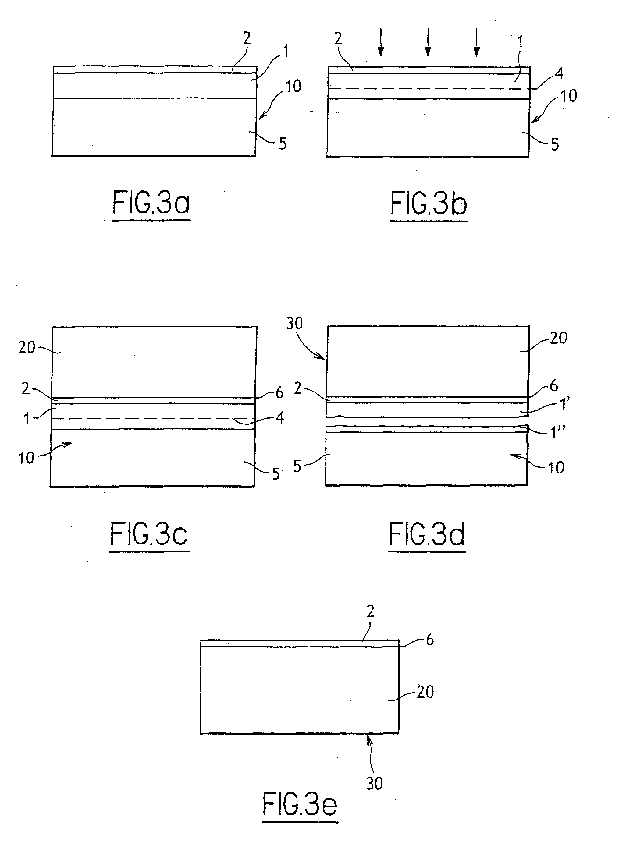
[0029] Presented are example embodiments of methods according to the invention, as well as applications based on the transfer of layers using the SMART-CUT® method with Type IV materials or alloys, and in particular with Si and SiGe.
[0030] The invention provides a number of improvements and advantages over prior art processes. The present methods reduce the duration, the economic cost and the number of treatments for the taken-off layer, and in particular to avoid using mechanical polishing. It also seeks to avoid delamination of the edge of the bonding layer when the finishing chemical etching takes place. Thus, the method can be used to create a structure, such as a semiconductor on insulator structure, comprising a taken-off layer including more weak material than Si, such as strained Si or SiGe, from a sampled layer of better quality material. Another benefit is that the quantity of material wasted when treating the taken-off layer is reduced. Thus, the invention proposes a sim...
PUM
 Abstract
Description
Claims
Application Information