
Semiconductor device with pins and method of assembling the semiconductor device

a semiconductor device and semiconductor technology, applied in semiconductor devices, semiconductor/solid-state device details, cooling/ventilation/heating modifications, etc., can solve the problems of increasing the cost and increasing and the position of the pins to be moved, so as to facilitate the assembling work of the semiconductor device, the shape and the weight of the semiconductor device can be decreased.

Inactive Publication Date: 2005-11-10
FUJITSU LTD
View PDF7 Cites 8 Cited by
  • Summary
  • Abstract
  • Description
  • Claims
  • Application Information

AI Technical Summary

Benefits of technology

[0008] It is an object of the present invention to provide a semiconductor device which can be produced at a low cost and in which a heat sink can be secured to a substrate without using screws, and a method of assembling such a semiconductor device.
[0012] In this constitution, the heat sink and the substrate are assembled in a unit in close contact closely with each other by the pins and the springs. The pins are separated from each other and can be formed in the smallest shape. The pins are first arranged in the holding member, and therefore, the pins can be inserted at one time in the holes in the heat sink and the holes in the substrate while compressing the springs by the holding member. This facilitates the assembling work of the semiconductor device. The holding member is finally removed from the pins, and therefore, the shape and the weight of the semiconductor device can be decreased. The holding member can be repetitively used, and there is no need to provide many holding members.
[0013] In this manner, according to the present invention, the heat sink and the substrate can be closely contacted together, as a unit, by the pins and the springs, without using screws. In assembling the semiconductor device, the pins are handled in a state of being arranged on the holding member. After the semiconductor device is assembled, the holding member can be removed from the pins. It is therefore possible to obtain a semiconductor device having a compact outer shape.

Problems solved by technology

The structure for securing the heat sink to the substrate by using screws requires laborious work for attaching the screws, thus increasing the cost.
Therefore, holding members having a plurality of pins must be provided in a large number, resulting in an increase in the cost and an increase in the weight of the semiconductor device.
Besides, the movable engaging member may cause the position of the pins to be moved if an external force, such as vibration or shock, is exerted thereon.

Method used


Image

  • Semiconductor device with pins and method of assembling the semiconductor device
  • Semiconductor device with pins and method of assembling the semiconductor device
  • Semiconductor device with pins and method of assembling the semiconductor device

Examples


Embodiment Construction

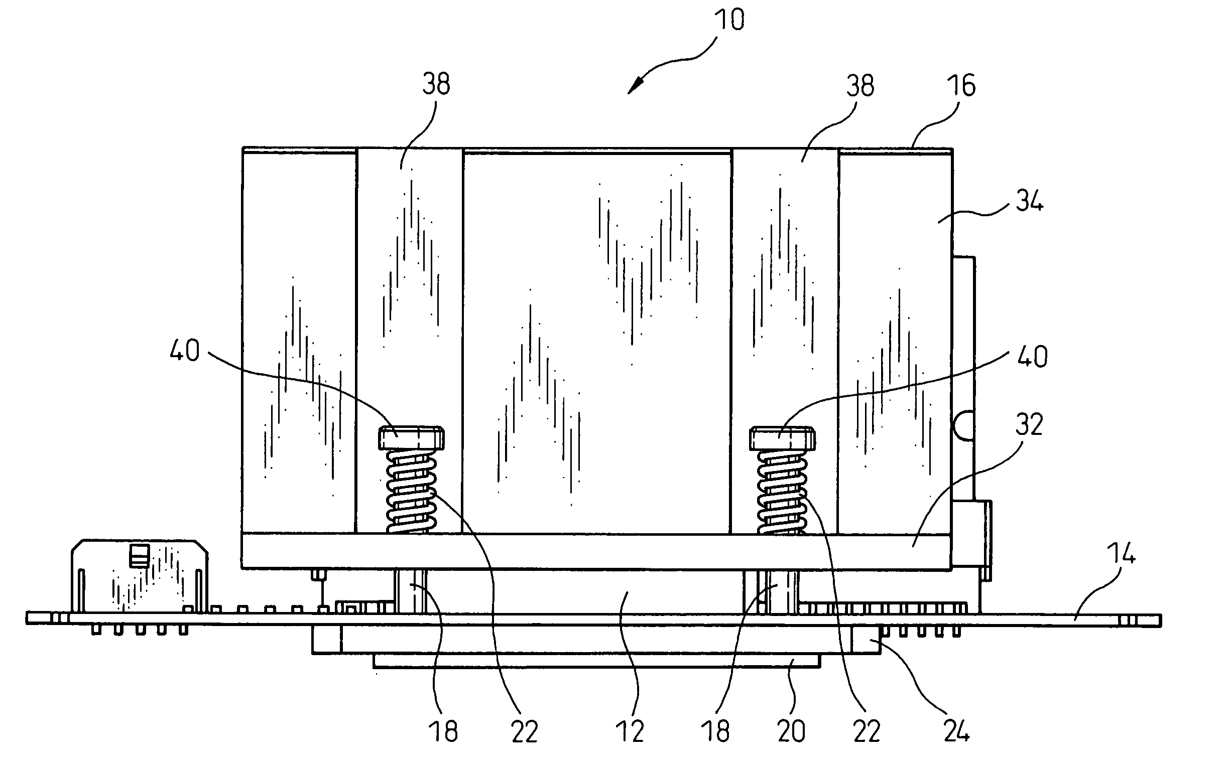
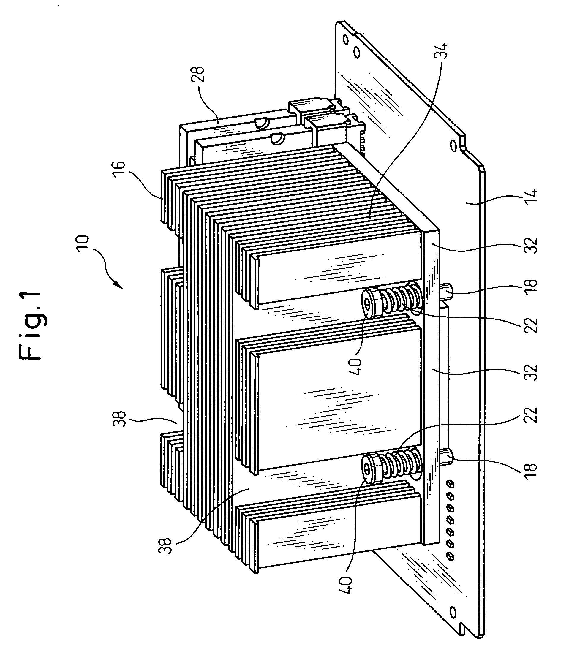
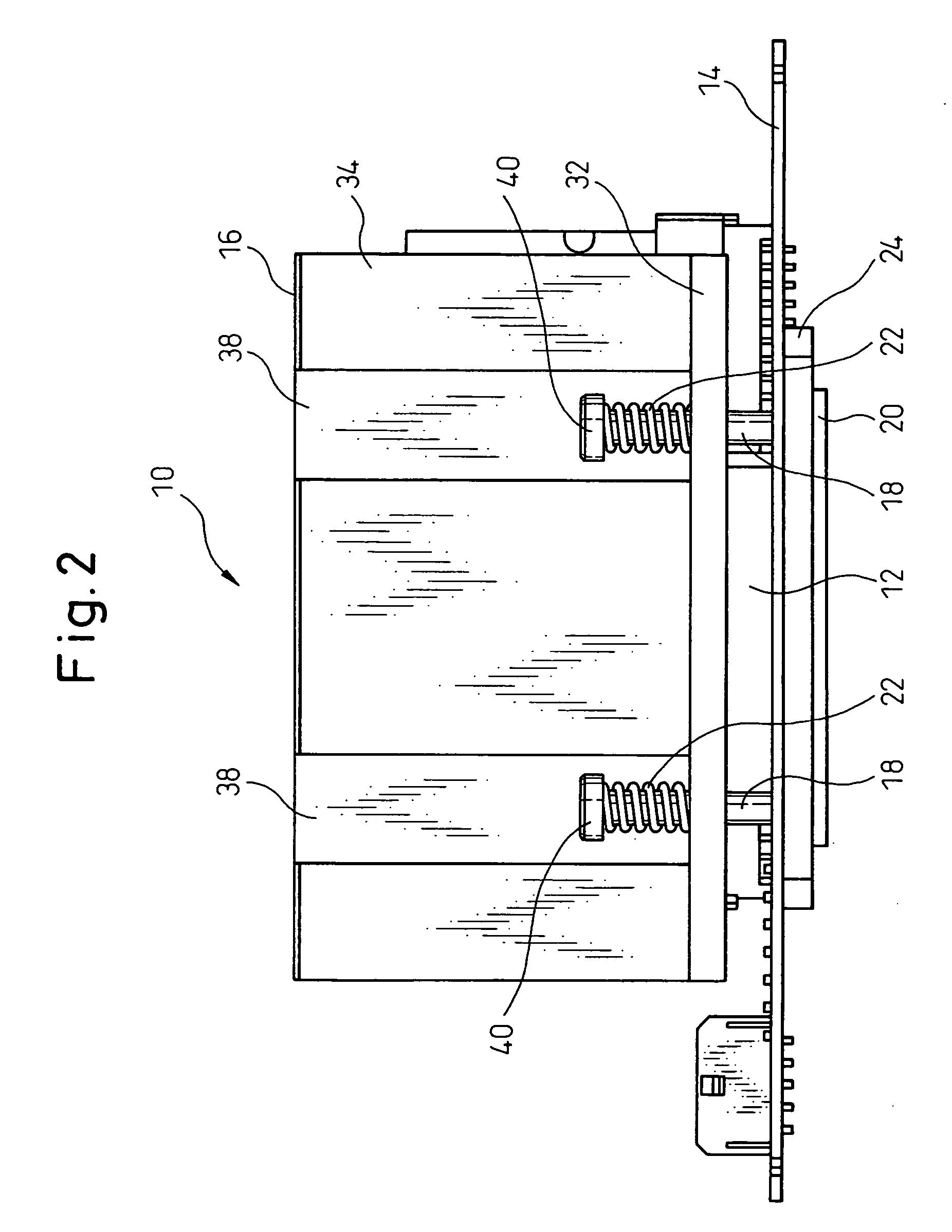
[0022] The preferred embodiment of the present invention will now be described with reference to the drawings. FIG. 1 is a perspective view illustrating a semiconductor device according to the embodiment of the present invention. FIG. 2 is a side view illustrating the semiconductor device of FIG. 1. FIG. 3 is a perspective view illustrating the semiconductor device in the state in which it is being assembled, as viewed from the lower side. FIG. 4 is an exploded perspective view illustrating the semiconductor device of FIG. 3.

[0023] The semiconductor device 10 comprises a substrate 14 having a semiconductor element 12 mounted thereon, a heat sink 16 in contact with the semiconductor element 12 to cool the semiconductor element 12, and a securing structure for securing the heat sink 16 to the substrate 14. The securing structure comprises a plurality of pins 18 that are inserted in a plurality of holes 36 in the heat sink 16 and in a plurality of holes 30 in the substrate 14 and havi...


PUM


Abstract

A semiconductor device includes a substrate having a semiconductor element mounted thereon, and a heat sink. A plurality of pins are inserted in holes in the heat sink and holes in the substrate to secure the heat sink to the substrate. The pin has an enlarged portion at one end thereof and an engaging portion at the other end thereof. An engaging member is provided to engage with the engaging portions of the pins that pass though the holes in the heat sink and the holes in the substrate and protrude from the substrate. Springs are arranged between the enlarged portions of the pins and the heat sink. In assembling the semiconductor device, the pins are held collectively by a holding member, and after the semiconductor device is assembled, the holding member is removed from the pins.

Description

BACKGROUND OF THE INVENTION [0001] 1. Field of the Invention [0002] The present invention relates to a semiconductor device and a method of assembling the semiconductor device. [0003] 2. Description of the Related Art [0004] In a semiconductor device including a semiconductor element that generates a large amount of heat such as a CPU, it is conventional to arrange a heat sink in contact with the semiconductor element to remove the heat generated by the semiconductor element. In many cases, the heat sink is secured by screws to the substrate on which the semiconductor element is mounted. [0005] The structure for securing the heat sink to the substrate by using screws requires laborious work for attaching the screws, thus increasing the cost. Therefore, a structure has been proposed for securing the heat sink to the substrate without using screws (see, for example, Japanese Registered Utility Model No. 3064402). [0006] In this prior art, a holding member has a plurality of pins colle...

Claims


Application Information

Patent Timeline
Patent Type & Authority Applications(United States)
IPC IPC(8): H01L21/44H01L23/40H01L23/48
CPCH01L23/4006H01L2023/4043H01L2023/405H01L2924/0002H01L2924/00
Inventor SO, TSUYOSHI
Owner FUJITSU LTD
Learn More