Electro-optic array interface

a technology of optical arrays and interfaces, applied in the field of interconnections, can solve the problems of limiting the application of optical waveguide light guides, affecting the performance of optical waveguides, and unable to fully exploit the ghz range, and the challenge of routing signals off-chip and into the system in the ghz frequency range is expected to exceed the challenge of achieving on-chip performan

Inactive Publication Date: 2005-11-10
CIENCIA
View PDF17 Cites 34 Cited by
  • Summary
  • Abstract
  • Description
  • Claims
  • Application Information

AI Technical Summary

Benefits of technology

[0015] The inventive electro-optic array interface may be electronically or optically addressable. That is, modulation of pixel reflectance may be achieved by directly applying an electrical signal to the control electrodes to provide an electrically addressable array. The microarray could also be implemented as an optically addressable device by connecting the control electrodes to the voltage source through photoconducting gates made from a photoconducting material, such as amorphous silicon (see FIG. 5). Addressing would then be accomplished by illuminating the appropriate photoconducting gates with a write beam. In this embodiment, chips containing laser diode arrays would provide the write beams for optical addressing of the modulator array.

Problems solved by technology

Performance in the GHz range can only be fully exploited if the off-chip interconnection technology provides appropriate bandwidth, a constraint that will become increasingly more severe during the next ten years.
This means that the challenge of routing signals off-chip and into the system in the GHz frequency range is expected to exceed that of achieving on-chip performance at these frequencies.
In addition, highly parallel, next-generation computational systems will require highly dense connection networks containing many long-distance connections.
In such highly connected, highly parallel systems, the module-to-module and long distance chip-to-chip connections are responsible for the majority of the power dissipation, time delay and surface area.
The reason is that the phase velocity of the surface plasmon is slower than that of light and therefore their wave vectors cannot be matched to achieve resonance.
The lack of grating-coupled systems has been primarily due to the greater complexity of fabrication that was previously required to make gratings.
Due to factors such as cost, physical size and additional necessary mounting hardware, the prism coupler is unsuitable for mass-produced, compact optical interconnects.

Method used


Image

  • Electro-optic array interface
  • Electro-optic array interface
  • Electro-optic array interface

Examples


Embodiment Construction

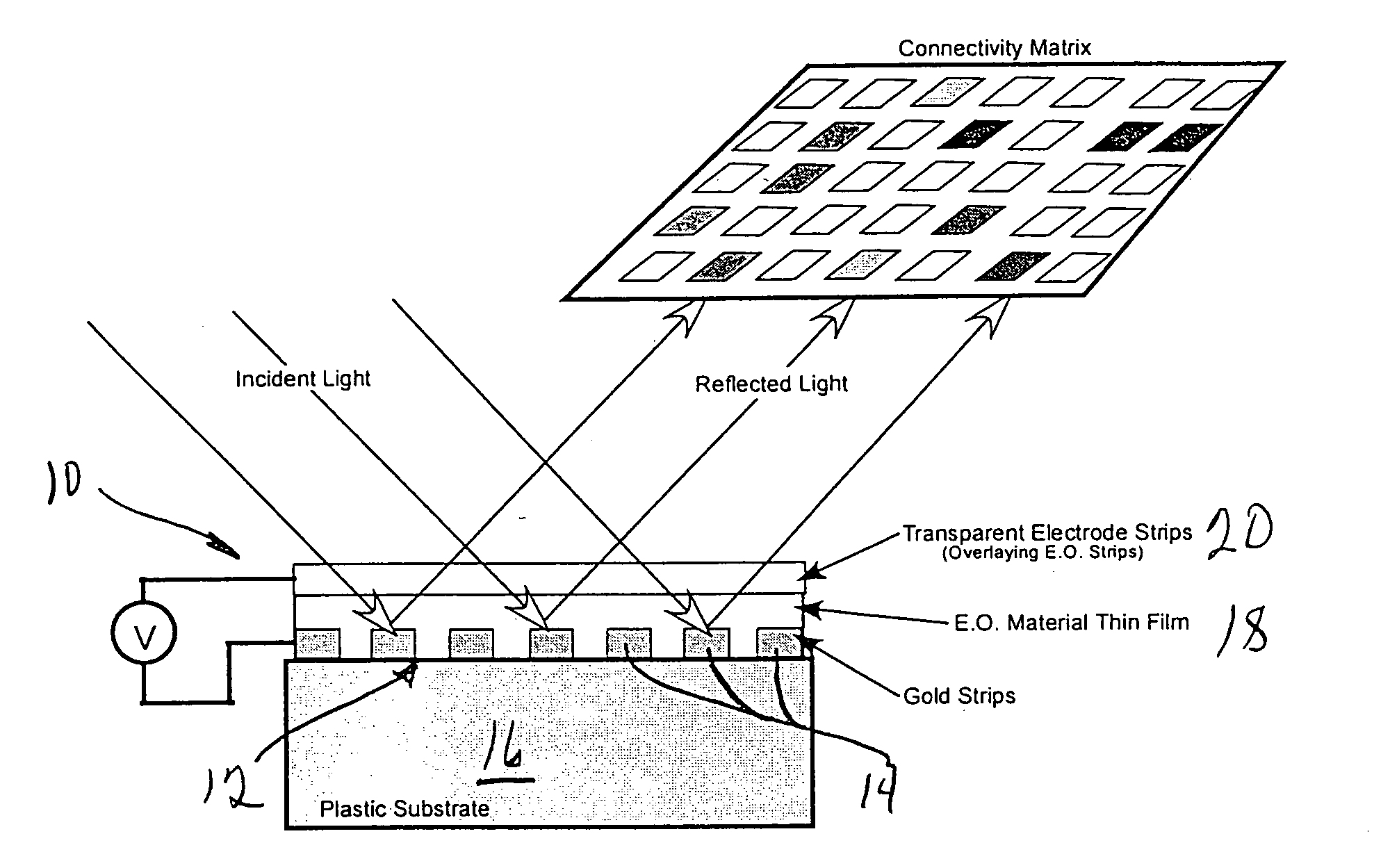
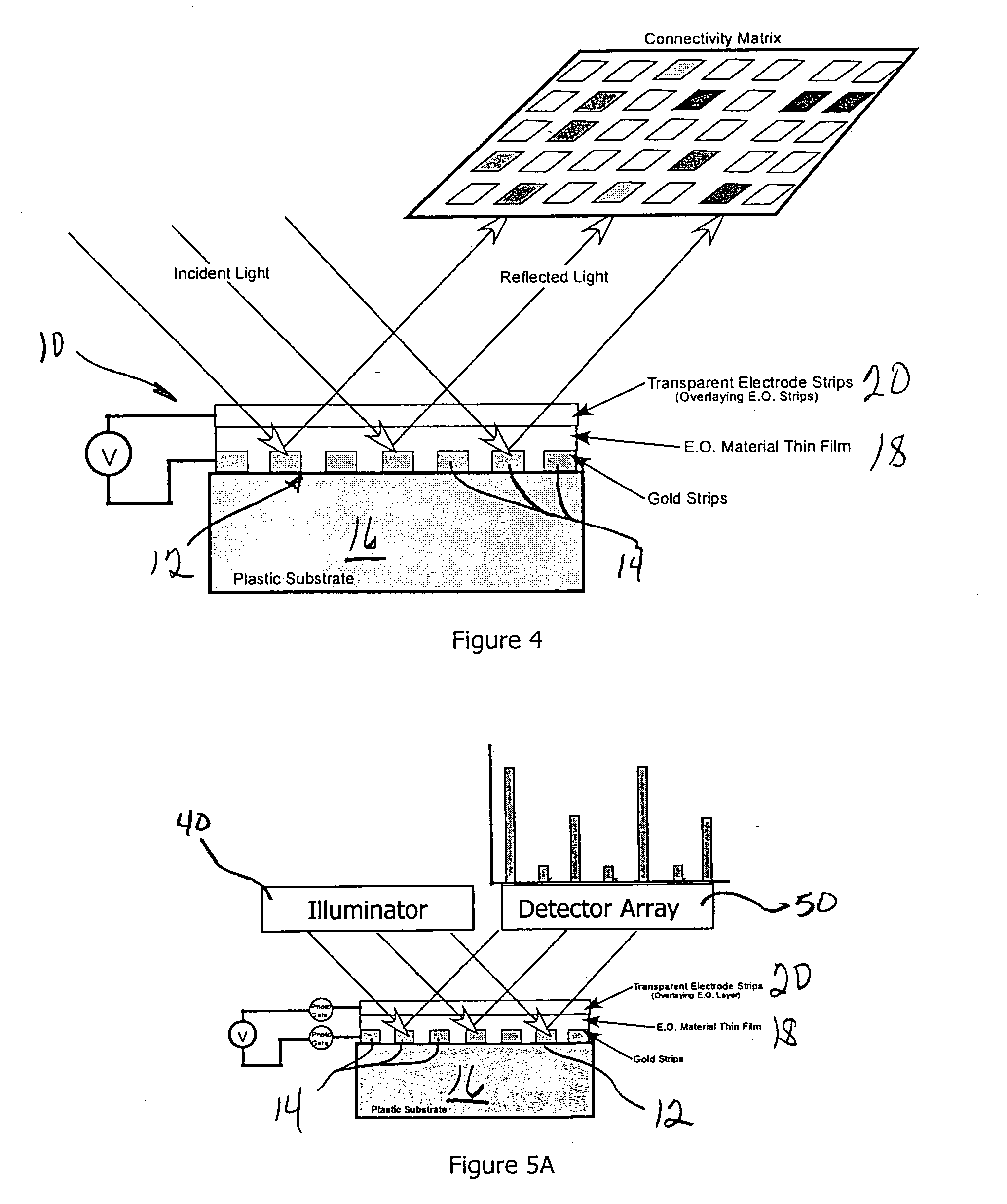
[0029] An embodiment of the electro-optic array interface 10 includes a diffraction grating 12 onto which a gold electrode array of strips 14 along the X-direction is deposited (the grating may be formed on a substrate material other than plastic, e.g. silicon or resin) as shown in FIGS. 4, 5A and 5B. In the context of the present invention, the diffraction grating 12 is a repeating pattern of parallel microgrooves on a dielectric substrate 16 such as plastic or silicon. The width of the gold electrodes 14 (exaggerated in FIGS. 4, 5A and 5B) should be of the order of the plasmon propagation length (˜20 μm). Above this gold array is deposited a thin film 18 of the EO polymer that forms the dielectric, and which should be at least 0.1 μm thick to maximize its interaction with the plasmon field. The inventors believe the thickness of the EO layer 18 can be optimized, with a goal of decreasing this thickness to allow the EO polymer layer 18 to be formed by self-assembly deposition techn...


PUM

PropertyMeasurementUnit
on-chip clock frequenciesaaaaaaaaaa
wavelengthaaaaaaaaaa

Abstract

A grating coupled surface plasmon resonance optical modulator is disclosed. A electro-optic polymer dielectric is deposited on the metallic surface of a diffraction grating to provide a metal/dielectric interface. A surface plasmon will propagate at the metal/dielectric interface in a resonant condition, e.g., when the metal surface is illuminated by transverse magnetic (TM) polarized light of the appropriate wavelength, angle of incidence and phase velocity. In the present invention, phase velocity is controlled by the diffraction grating. A transparent electrode deposited on the electro-optic layer allows an electrical potential to be applied across the electro-optic polymer. The applied electrical potential (voltage) changes the index of refraction of the electro-optic polymer, thereby disrupting the resonant condition to produce an optically detectable change in reflectance of incident light from the metal layer. The disclosed grating coupled surface plasmon resonance optical modulator may be configured as an electronically or optically addressable array.

Description

CROSS REFERENCE TO RELATED APPLICATIONS [0001] This application is a continuation-in-part of U.S. patent application Ser. No. 10 / 842,366, filed May 10, 2004.STATEMENT REGARDING FEDERALLY SPONSORED RESEARCH OR DEVELOPMENT [0002] This invention was made with United States Government support under grant number DMI0215098. The United States Government has certain rights to this invention.FIELD OF THE INVENTION [0003] The present invention relates generally to interconnections between electronic chips or devices and more specifically to an electro-optic modulator for use as an interface between electronic components and optical communication pathways. BACKGROUND OF THE INVENTION [0004] At present, microprocessors are providing on-chip clock frequencies on the order of 1 GHz. The International Technology Roadmap for Semiconductors (ITRS) forecasts on-chip clock rates of about 10 GHz in 2011. Performance in the GHz range can only be fully exploited if the off-chip interconnection technolog...

Claims


Application Information

Patent Timeline
Patent Type & Authority Applications(United States)
IPC IPC(8): G02B6/10G02B6/122G02F1/00G02F1/03G02F1/061G02F1/07
CPCB82Y20/00G02B6/1226G02F2203/10G02F2201/307G02F1/061
Inventor SAWIN, RAYFERNANDEZ, SALVADOR M.
Owner CIENCIA
Why Eureka
Try Eureka