Method and apparatus for automated debug and optimization of in-circuit tests

a technology of in-circuit tests and automated debugging, applied in the direction of testing circuits, nuclear elements, instruments, etc., can solve the problems of large number of manual repair of tests, large number of tests that cannot be determined by test, and increased cost and complexity of designing and testing these integrated circuits

Inactive Publication Date: 2005-11-10
AGILENT TECH INC
View PDF6 Cites 14 Cited by
  • Summary
  • Abstract
  • Description
  • Claims
  • Application Information

AI Technical Summary

Benefits of technology

[0004] The present invention is a method and apparatus for automatically debugging and optimizing an in-circuit test that is used to test a device under test on an automated tester is presented. The novel test debug and optimization technique extracts expert knowledge contained in a knowledge framework and automates the formulation of a valid stable test for execution on an integrated circuit tester. In accordance with the invention, an in-circuit tester includes an automated test debug and optimization system which receives an integrated circuit test and performs debug and preferably optimization of the test to ensure that the test will meet at least validity and stability requirements. The automated test debug and optimization system includes an autodebug controller, which has a test formulation engine that accesses a knowledge framework associated with the device under test to formulate and package a valid stable, and preferably optimal, test for testing the device under test. The autodebug controller iterates through a number of rules associated with an active ruleset corresponding to the component to be tested by the test. The rules define actions and validation criteria, and preferably stability criteria. A newly formulated proposed test is generated based on a given rule and tested on the test head to establish whether the proposed test meets the validation criteria, and preferably the stability criteria. Once a proposed test has been found that meets the required criteria, it is preferably used to replace the originally presented test. If optimization is to be performed, the autodebug controller generates all possible proposed tests based on the knowledge framework, and selects the proposed test that best meets the validation and stability criteria.

Problems solved by technology

With the improvements in speed and density of integrated circuits, the cost and complexities of designing and testing these integrated circuits has dramatically increased.
However, for various reasons, frequently a fairly significant percentage (e.g., 20%) of the automatically generated tests are faulty in that when executed on a known good device under test, the test is unable to determine the status of the device or component under test.
Clearly, for devices under test that include thousands of components, this results in a large number of tests that must be manually repaired.
However, with such a large number of “broken” tests to repair, a large (and therefore, very costly) amount of time can be spent in test debug and optimization, rather than spent in actual testing of the device itself.

Method used


Image

  • Method and apparatus for automated debug and optimization of in-circuit tests
  • Method and apparatus for automated debug and optimization of in-circuit tests
  • Method and apparatus for automated debug and optimization of in-circuit tests

Examples


Embodiment Construction

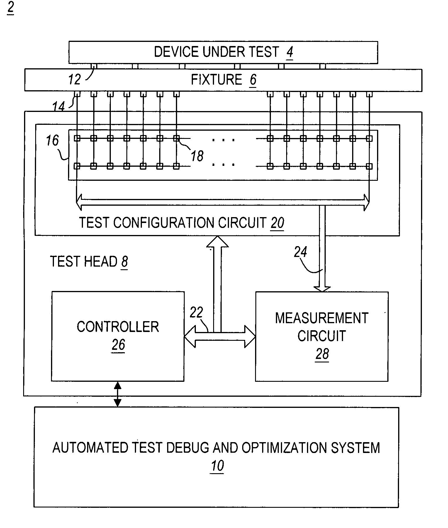
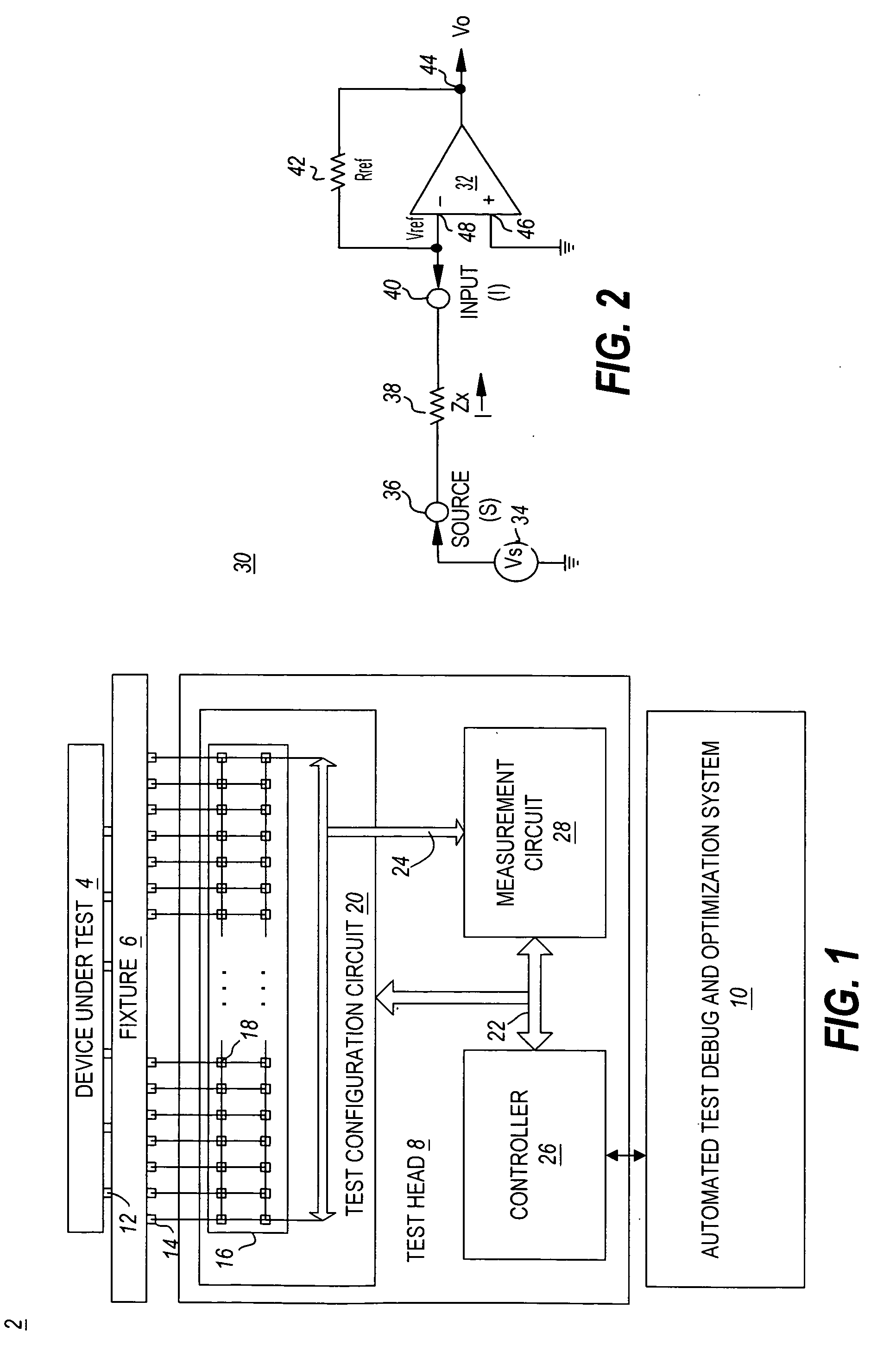
[0013] Turning now to the invention, FIG. 1 is a schematic block diagram of an automated test system 2 implemented in accordance with the invention. As illustrated, test system 2 includes a test head 8 which supports a fixture 6 on which a printed circuit board (PCB) containing or implementing a device under test (DUT) 4 is mounted, and an automated test debug and optimization system 10. The test head 8 includes a controller 26, a test configuration circuit 20, and a measurement circuit 28. Fixture 6, for example a bed-of-nails fixture, is customized for each PCB layout and includes a plurality of probes 12 that electrically connect to nodes of the device under test 4 when the device under test 4 is properly seated on the fixture 6. Probes 12 are coupled via the fixture 6 to interface pins 14.

[0014] The test configuration circuit 20 includes a matrix 16 of relays 18 which is programmable via controller 26 over control bus 22 to open and / or close each relay 18 in the matrix 16 to ac...


PUM


Abstract

A method and apparatus for automatically debugging and optimizing an in-circuit test that is used to test a device under test on an automated tester is presented. The novel test debug and optimization technique extracts expert knowledge contained in a knowledge framework and automates the formulation of a valid stable, and preferably optimized, test for execution on an integrated circuit tester.

Description

BACKGROUND OF THE INVENTION [0001] The increasing reliance upon computer systems to collect, process, and analyze data has led to the continuous improvement of the system assembly process and associated hardware. With the improvements in speed and density of integrated circuits, the cost and complexities of designing and testing these integrated circuits has dramatically increased. Currently, large complex industrial integrated circuit testers (commonly referred to in the industry as “Automated Test Equipment” or “ATE”) perform complex testing of integrated circuit devices, such as integrated circuits, printed circuit boards (PCBs), multi-chip modules (MCMs), System-on-Chip (SOC) devices, printed circuit assemblies (PCAs), etc. The tests that must be performed may include, among others, in-circuit test (ICT), functional test, and structural test, and are designed to verify proper structural, operational, and functional performance of the device under test (DUT). [0002] An example of...

Claims


Application Information

Patent Timeline
Patent Type & Authority Applications(United States)
IPC IPC(8): G01R31/28G01R31/3183G06F11/00G06F11/25H01T13/60
CPCG06F11/2257G01R31/31835
Inventor LOH, AIK KOONWAI, KEEN FUNGTAN, TIAM HOCKWILLIAMS, ROY H.
Owner AGILENT TECH INC
Why Eureka
Try Eureka