Semiconductor device and method for fabricating the same

Inactive Publication Date: 2005-11-17
FUJITSU LTD
View PDF0 Cites 19 Cited by
  • Summary
  • Abstract
  • Description
  • Claims
  • Application Information

AI Technical Summary

Benefits of technology

[0011] According to the present invention, by the first thermal processing, a part of a relatively thick nickel film on the lower side and a part of a silicon substrate on the upper side are reacted with each other, whereby in the first thermal processing, an Ni2Si film can be formed while the formation of NiSi2 crystals is suppressed. Then, in the present invention, a part of the nickel film, which has not reacted with the Si is selectively etched off, and then, by the second thermal processing the Ni2Si film and a part of the silicon substrate on the upper side are reacted with each other to form an NiSi film, whereby the NiSi film is prevented

Problems solved by technology

However, when the silicidation is performed with Ni film simply used, the roughness of the interface between the silicon layer and silicide film is

Method used


Image

  • Semiconductor device and method for fabricating the same
  • Semiconductor device and method for fabricating the same
  • Semiconductor device and method for fabricating the same

Examples


Example

A First Embodiment

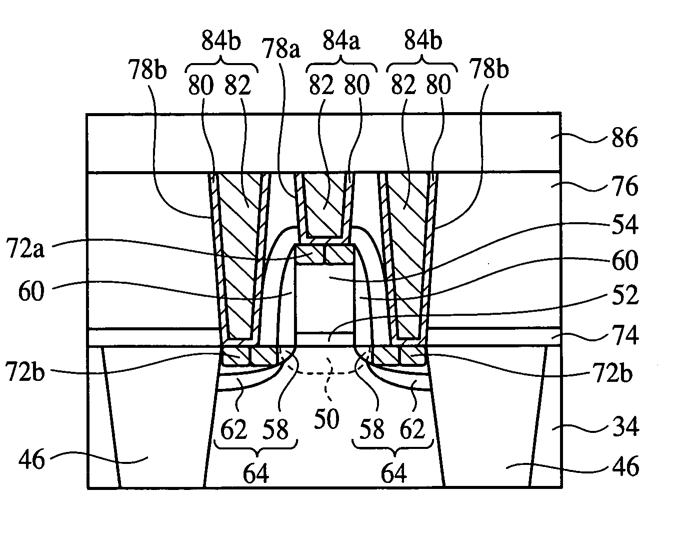
[0072] The semiconductor device according to a first embodiment of the present invention and the method for fabricating the same will be explained with reference to FIGS. 7 to 22. FIG. 7 is a sectional view of the semiconductor device according to the present embodiment. FIGS. 8A-8C to 18A-18C are sectional views of the semiconductor device according to the present embodiment in the steps of the method for fabricating the semiconductor device, which illustrate the method. FIGS. 19A-19D are transmission electron microscopic pictures showing the results of evaluating the method for fabricating the semiconductor device according to the present embodiment. FIG. 20 is a sectional view of the semiconductor device used in evaluating the method for fabricating the semiconductor device according to the present embodiment, which shows the structure thereof. FIGS. 21 and 22 are graphs of the results of evaluating the method for fabricating the semiconductor device according ...

Example

[0149] In contrast to these, in Example 1 shown in FIG. 19A, such NiSi2 crystals were not observed. That is, in Example 1, the nickel silicide film formed on the source / drain diffused layer is formed of nickel silicide alone of the NiSi phase alone.

[0150] As evident from the comparison among the electron microscopic pictures, it is found that the roughness in the interface between the source / drain diffused layer 88 and the NiSi film 90 is much small in Example 1 in comparison with Controls 1 to 3.

[0151] Based on the above-described result of the sectional observation with a transmission electron microscope, the method for fabricating the semiconductor device according to the present embodiment can form the NiSi film of good quality while suppressing the formation of the NiSi2 film, and it has been confirmed that the roughness in the interface between the silicon substrate and the NiSi film can be decreased.

[0152] (Evaluation Result (Part 2))

[0153] The junction leak current of th...

Example

[0155] In FIG. 21, the ▾ marked plots indicate the measured result of Example 2, i.e., the method for fabricating the semiconductor device according to the present embodiment. In Example 2, a TiN film is formed on a 20 nm-thickness Ni film, and the first thermal processing was performed at 270° C. for 30 seconds. Next, the TiN film and the part of the Ni film, which had not reacted with the Si, were selectively removed by cleaning with ammonia / hydrogen peroxide mixture and sulfuric acid / hydrogen peroxide mixture, and then the second thermal processing was performed at 500° C. for 30 seconds.

[0156] In FIG. 21, the ● marked plots indicate the measured result of Control 4 in which a relatively thin Ni film was formed, and the thermal processing was performed once. In Control 4, a TiN film was formed on a 10 nm-thickness Ni film, and the thermal processing was performed once at 400° C. for 30 seconds. Then, the TiN film and the part of the Ni film, which had not reacted with the Si wer...


PUM


Abstract

The method for fabricating a semiconductor device comprises the step of forming an Ni film 66 on a source/drain diffused layers 64, the first thermal processing step of reacting a part of the Ni film 66 on the lower side and a part of the source/drain diffused layers 64 on the upper side with each other by thermal processing to form Ni2Si films 70b on the source/drain diffused layers 64, and the step of etching off the part of the Ni film 66, which has not reacted, and the second thermal processing of reacting by thermal processing the Ni2Si films 70b and parts of the source/drain diffused layers 64 on the upper side with each other.

Description

CROSS-REFERENCE TO RELATED APPLICATIONS [0001] This application is based upon and claims priorities of Japanese Patent Application No. 2004-146763, filed on May 17, 2004, and Japanese Patent Application No. 2004-294855, filed on Oct. 7, 2004, the contents being incorporated herein by reference. BACKGROUND OF THE INVENTION [0002] The present invention relates to a semiconductor device and a method for fabricating the same, more specifically, a semiconductor device and a method for fabricating the same in which silicidation using nickel is performed. [0003] As a technique of making gate electrodes and source / drain diffused layers less resistive is known the so-called salicide (Self-Aligned Silicide) process for forming metal silicide film by self-alignment on the surfaces of the gate electrode and the source / drain diffused layers. As a metal material which is reacted with silicon in the salicide process, cobalt (Co) is widely used (refer to, e.g., Japanese published unexamined patent ...

Claims


Application Information

Patent Timeline
IPC IPC(8): H01L21/28H01L21/285H01L21/336H01L29/417H01L29/423H01L29/49H01L29/76H01L29/78
CPCH01L21/28518H01L29/6659H01L29/665H01L21/76897H01L21/823814
Inventor KAWAMURA, KAZUO
Owner FUJITSU LTD
Why Eureka
Try Eureka