Solder flow stops for semiconductor die substrates
- Summary
- Abstract
- Description
- Claims
- Application Information
AI Technical Summary
Benefits of technology
Problems solved by technology
Method used
Image
Examples
Embodiment Construction
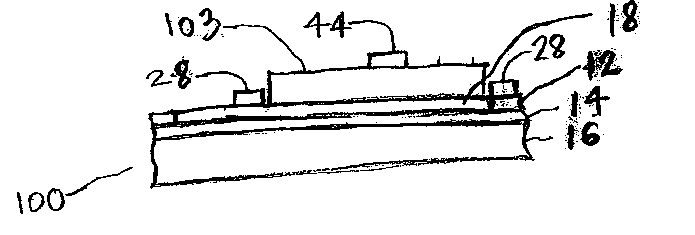
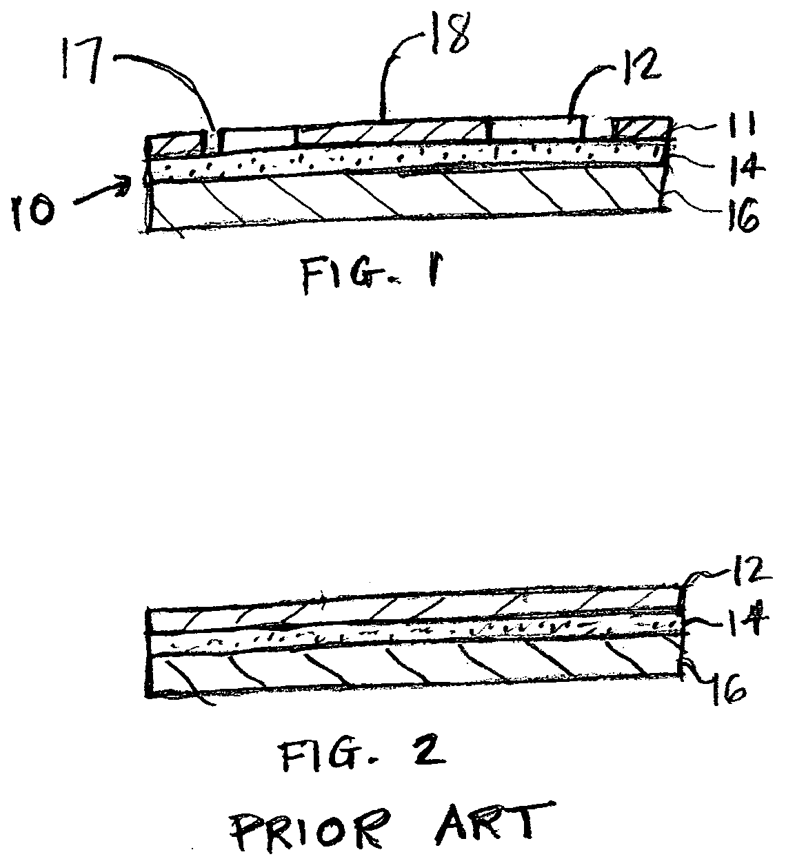
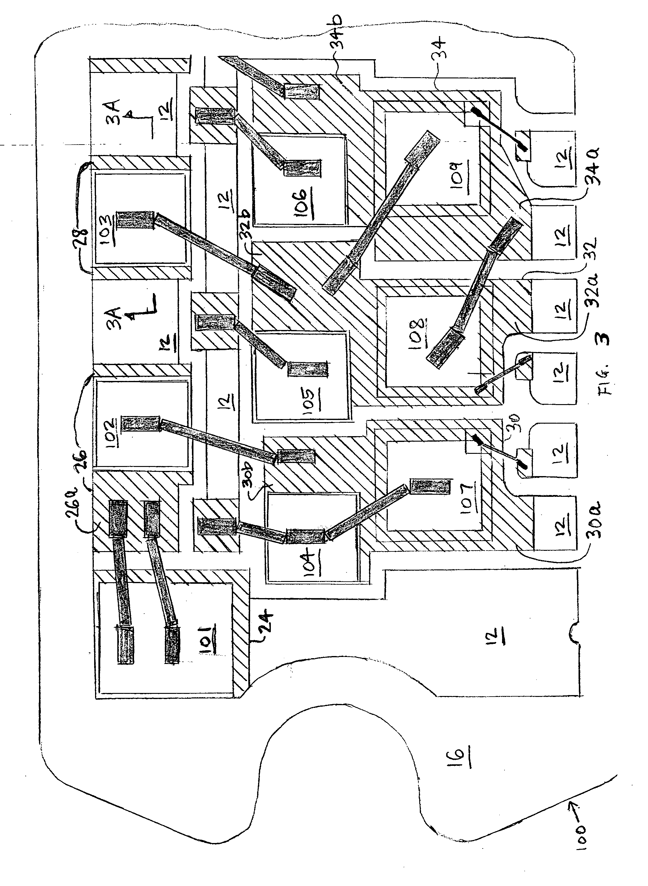
[0016]FIG. 1 illustrates one embodiment of the present invention. A solder flow stop 11 surrounds a copper mounting pad 18, which is etched out of copper layer 12, on the surface of an insulated metal substrate 10. Flow stop 11 can be aluminum, which is non-wetting to a solder of tin-lead. Aluminum is also used for the flow stops 24, 26, 28, 30, 32, 34 in FIG. 3; however, any material that is non-wetting to the solder and circuit layer 12 during the solder reflow process may be used as the solder flow stop. Non-wetting means that the material is comparatively non-wetting with respect to the material of circuit layer 12 (copper) and the solder, such that the solder tends to stay on the mounting pad 18. Aluminum is a preferred material for this solder and circuit layer 12 combination. Other solder flow stop materials may be preferred for other combinations of solder and circuit layer 12 material.
[0017] Solder metals which can be used include tin-lead, tin-lead-silver, tin-antimony, l...
PUM
 Abstract
Description
Claims
Application Information


