Circuit with at least one delay cell

Inactive Publication Date: 2005-11-17
ATMEL GERMANY
View PDF19 Cites 2 Cited by
  • Summary
  • Abstract
  • Description
  • Claims
  • Application Information

AI Technical Summary

Benefits of technology

[0026] A particular advantage of the invention is that a ring oscillator can also be implemented with an even number of delay cells that is greater than or equal to four. In contrast, the prior art is only capable of having ring oscillators with an odd number of delay cells. Since every delay cell with the features of the invention permits coupling out of two signals with complementary phases, the invention makes it possible to design ring oscillators which provide practically any even number of mutually phase-shifted signals with a minimum number of delay cells. In contrast, the prior art, which requires an odd number of delay cells to produce oscillation in the ring oscillator, provides only 6, 10, 14, . . . possibilities for coupling out signals if it is assumed that two signals can be coupled out per delay cell.
[0027] Also, at least one controllable source of electrical energy can be connected to the supply connections of at least one of the inverters.
[0028] As a resu

Problems solved by technology

Consequently, at high frequencies there is always the danger that the two inverter chains will not run synchronously.
However, such a differential stage is slower than an inverter since the gate drive voltage is lower.
Thus, in

Method used


Image

  • Circuit with at least one delay cell
  • Circuit with at least one delay cell
  • Circuit with at least one delay cell

Examples


Embodiment Construction

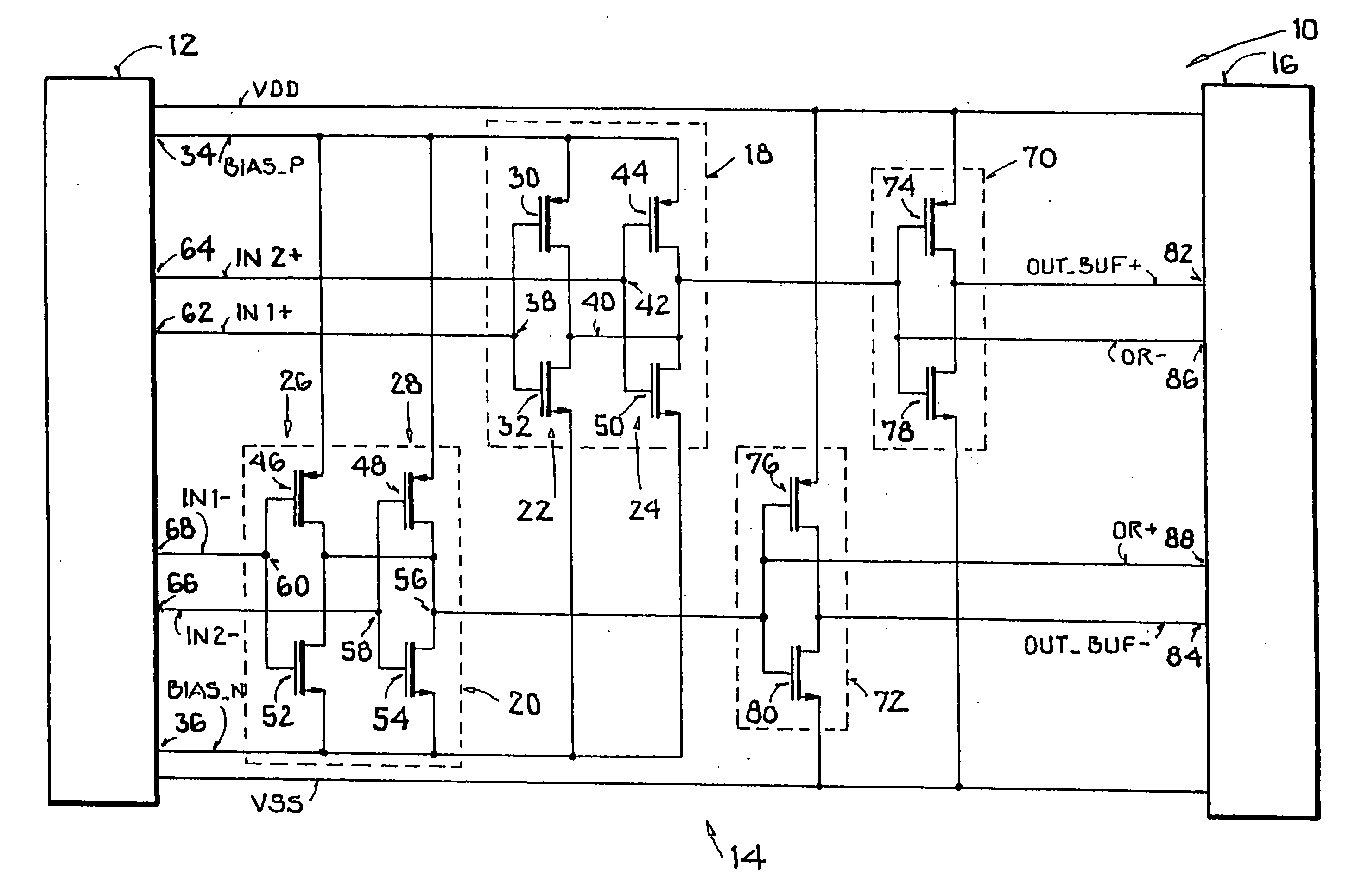
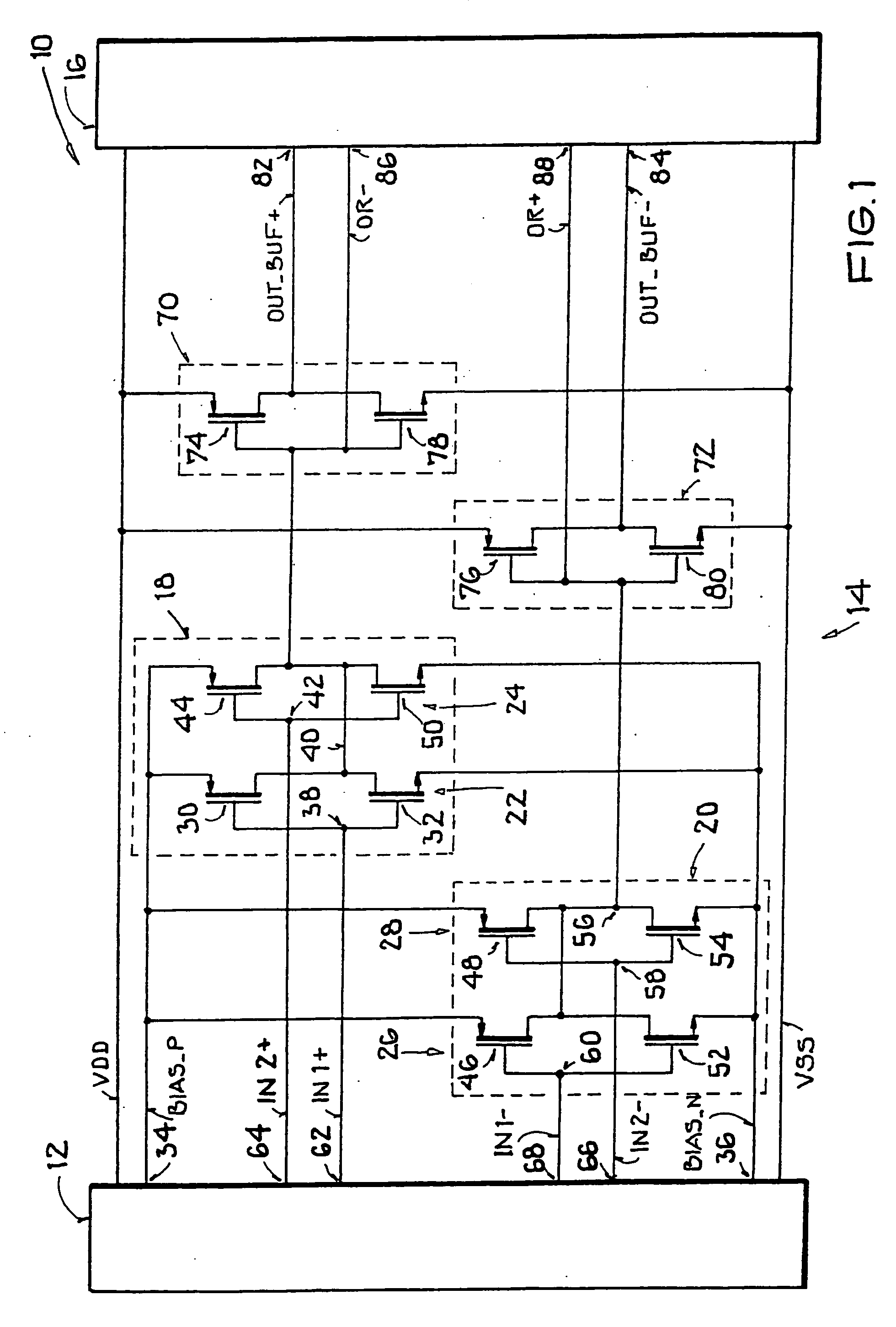
[0038] In particular, FIG. 1 shows a circuit 10 having an input circuit 12, a delay cell 14, and an output circuit 16. The delay cell 14 has two pairs 18, 20 of inverters 22, 24 and 26, 28. A first inverter 22 of the first pair 18 is preferably constructed as a CMOS inverter from a PMOS field-effect transistor 30 and an NMOS field-effect transistor 32 whose channels are located between a connection 34 with positive electrical potential BIAS_P and a connection 36 with negative electrical potential BIAS_N. When the gate connection 38, which serves as an input of the inverter 22, is driven with a positive potential, the channel of the NMOS transistor 32 conducts and the channel of the PMOS transistor 30 is turned off. As a result, the negative potential of the connection 36 is established at the output 40 of the inverter 22. Conversely, in the event of a negative potential at the gate connection 38, which results in a turned-off NMOS transistor 32 and conducting PMOS transistor 30, the...


PUM


Abstract

A circuit having at least one delay cell that reflects an input signal change in an output signal with a delay and that has at least two pairs of inverters, wherein the outputs of the inverters of each pair of inverters are connected to one another so that the connected outputs of a first pair of inverters form a first output of the delay cell and the connected outputs of a second pair form a second output. The circuit is characterized in that one input of each inverter is connected to its own input of the delay cell, separately from inputs of other inverters.

Description

[0001] This nonprovisional application claims priority under 35 U.S.C. § 119(a) on German Patent Application No. DE 102004025386.2, which was filed in Germany on May 17, 2004, and which is herein incorporated by reference. BACKGROUND OF THE INVENTION [0002] 1. Field of the Invention [0003] The present invention relates to a circuit with at least one delay cell that reflects an input signal change in an output signal with a delay and that has at least two pairs of inverters, wherein the outputs of the inverters of each pair of inverters are connected to one another so that the connected outputs of a first pair of inverters form a first output of the delay cell and the connected outputs of a second pair form a second output. [0004] 2. Description of the Background Art [0005] Delay cells are used, for example, to produce electrical oscillations in a voltage-controlled or current-controlled oscillator or for delayed forwarding of an input signal change in a signal processing circuit. [0...

Claims


Application Information

Patent Timeline
IPC IPC(8): H03K3/03H03K3/354H03K5/13H03K19/0948
CPCH03K3/0322
Inventor KARTHAUS, UDO
Owner ATMEL GERMANY
Why Eureka
Try Eureka