Light-guide module having light shielding structure

a lightguide module and light shielding technology, applied in optics, instruments, electrical appliances, etc., can solve the problems of black shadows, inconvenient installation, and inability to meet the requirements of high-resolution images, so as to reduce the cost, increase the assembly yield of the reflected mirror, and facilitate installation

Active Publication Date: 2005-11-17
INTELLECTUAL VENTURES I LLC
View PDF13 Cites 8 Cited by
  • Summary
  • Abstract
  • Description
  • Claims
  • Application Information

AI Technical Summary

Benefits of technology

[0011] Accordingly, it is an object of the present invention to provide a light shielding structure for reflected mirrors that can cover the excessive area of the reflected mirrors so that light reflected to the covered area is absorbed without directing to the image sensing device.
[0012] It is another object of the present invention to provide a light shielding structure that is easy to install on the excessive area of the reflected mirrors to reduce cost and increase assembly yield of the reflected mirrors.
[0013] It is yet another object of the present invention to maintain the original size of the reflected mirrors and provide a light shielding structure only on the excessive area to prevent erratic light reflection. As the dimension of the reflected mirrors is not altered, there is no need to change the configuration and calibration of the reflected mirrors, and redesign of the light-guide module is not necessary.
[0014] In one aspect, the invention provides a scanning apparatus to scan an image object. The scanning apparatus includes a light source, an image sensing device and a light-guide module. The light source aims to generate light to project to the image object and to be reflected thereof. The light-guide module includes at least one reflected mirror to transmit the reflecting light to the image sensing device. The image sensing device receives the light and generates corresponding digital signals. The reflected mirror includes a light shielding structure to prevent erratic light from occurring to the reflected mirror and directing to the image sensing device.
[0015] The present invention provides a simple design that couples a light shielding stricture on the excessive area of the original reflected mirror to absorb the erratic light or noise signals. It overcomes the conventional problems of adopting small reflected mirrors that results in a higher cost and difficult fabrication and assembly.

Problems solved by technology

As a result, the scan image generated by the conventional scanning device 10 often is blurred by black shadows or noise signals.
All this erratic reflection will generate redundant scanning images on the conventional scanning device 10 and result in undesirable scanning quality.
This becomes even more serious in the high resolution.
In addition, in the event of the calibration of the reflected mirrors is not properly done such as the one shown in FIG. 1 (not accurate positioning of the reflected mirrors), even if the light is projected to the center area of the reflected mirror, the reflected light could deviate and cannot travel on the correct light route and project correctly to the reflected mirrors at the later stages.
While the light might finally be reflected to the light sensing device, it is not a normal reflection and redundant scan images occur.
However, due to fabrication technique and material constraints, there is a limitation for the dimension of the reflected mirrors.
It is very difficult to produce reflected mirrors that fully meet the requirements.
As the prevailing trend of product design demands compact size, to shrink the size of the reflected mirrors often result in mirror shattering and higher cost.
Production and assembly become more complicated.
Any damage of the reflected mirrors will increase the fabrication cost and time.
When the reflected mirrors are too small, calibration of the reflected mirrors to form a correct light route also is more difficult.

Method used


Image

  • Light-guide module having light shielding structure
  • Light-guide module having light shielding structure
  • Light-guide module having light shielding structure

Examples


Embodiment Construction

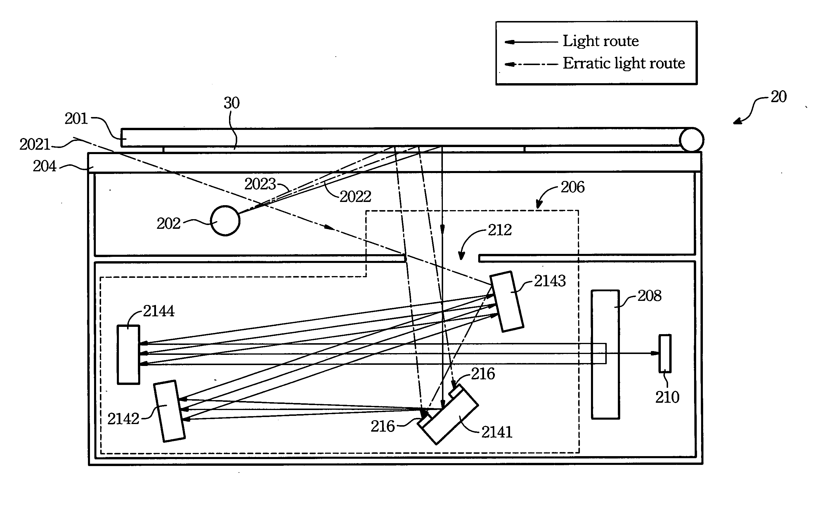
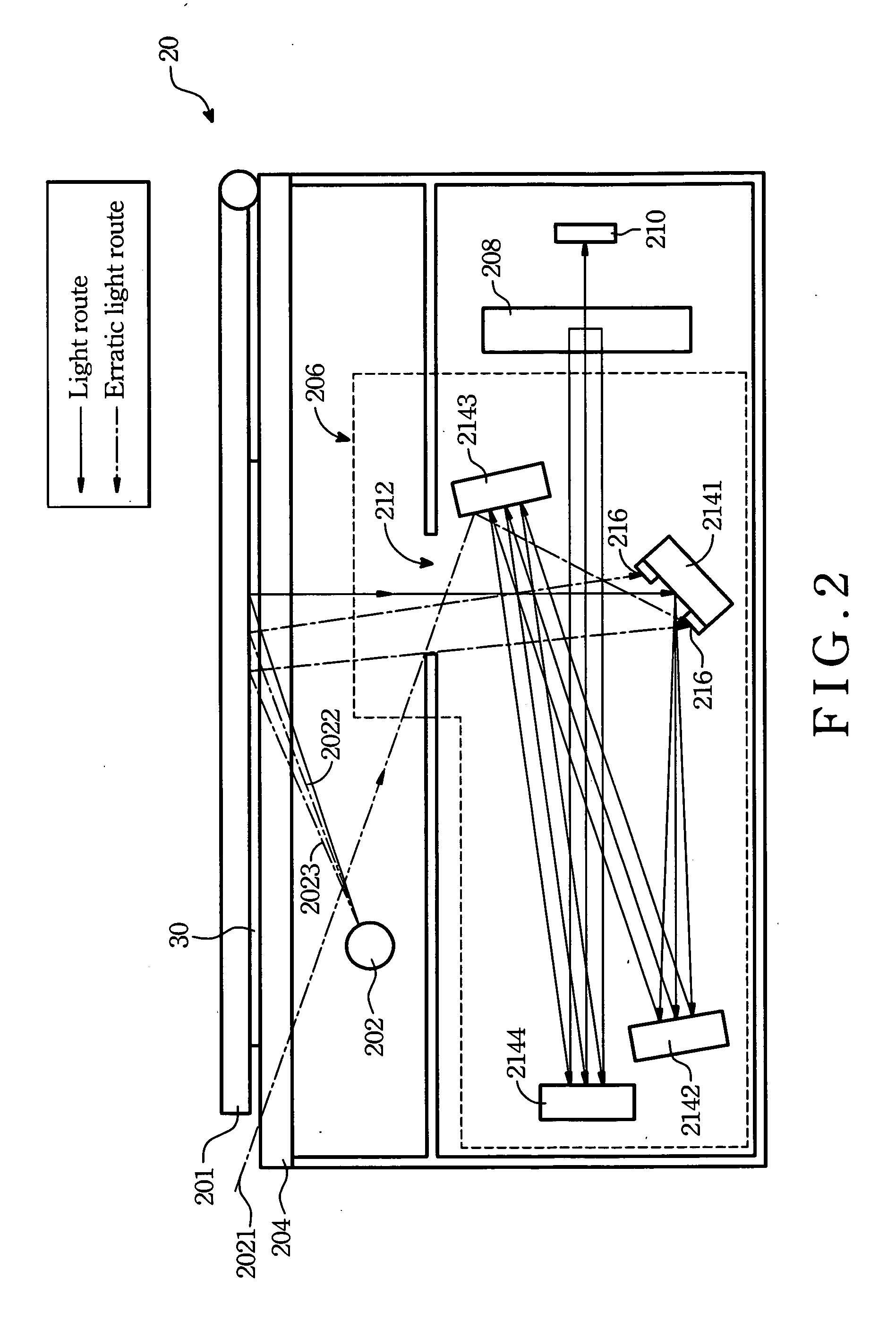
[0022] The light-guide module of the invention is adopted for use on an image processing device that has to direct or change the light traveling route such as a scanning device or MFP. The light-guide module mainly aims to receive light from an entrance and reflect the light through reflected mirrors to an image sensing device. Namely, the reflected mirrors in the light-guide module can alter the traveling route of the light to reduce the size of the device. The following embodiment is based on adopting the invention to a scanning apparatus.

[0023] Referring to FIG. 2, the scanning apparatus 20 includes a cover plate 201, a light source 202, a scanning deck 204, a light-guide module 206, a lens 208 and an image sensing device 210. The cover plate 201 aims to cover a scanning object 30 on the scanning deck 204. The light source 202 emits, light to the scanning object 30. The light is reflected by the scanning object 30. The scanning deck is made of glass and can withstand the weight ...


PUM


Abstract

A light-guide module is used for guiding the incident light to a process device. The light-guide module comprises an entrance and a plurality of reflected mirrors. The entrance is provided for entering the signal light. The reflected mirrors are arranged as a predetermined light route for guiding out the signal light. One of the reflected mirrors comprises a light shielding structure for preventing the noise reflecting from the reflected mirror so as to prevent the noise light from entering the image sensing device and to prevent the image sensing device to process the noise.

Description

BACKGROUND OF THE INVENTION [0001] (1) Field of the Invention [0002] The invention relates to a light shielding structure adopted for use on reflected mirrors, and more particularly to a light shielding structure for a light-guide module of an image scanning apparatus or a multi-functional peripheral to prevent redundant light reflection of reflected mirrors of the light-guide module or noise signals from projecting to an image sensing device. [0003] (2) Description of the Prior Art [0004] Under the present demand for improving image resolution and shrinking device size, there is a constant requirement for image process apparatus (such as scanners or MFPs) to adopt an advanced design in the optical processing mechanism that generates digital image signals. [0005] Refer to FIG. 1 for a conventional scanning device 10. It includes a cover plate 101, a light source 102, a scanning deck 104, a light-guide module 106, a lens 108 and an image sensing device 110. The cover plate 101 aims t...

Claims


Application Information

Patent Timeline
Patent Type & Authority Applications(United States)
IPC IPC(8): G02B5/00G02B26/10G02B27/00H04N1/00H04N1/04
CPCG02B5/005H04N2201/0458H04N1/00525G02B27/0018
Inventor CHEN, HSI-YU
Owner INTELLECTUAL VENTURES I LLC
Why Eureka
Try Eureka